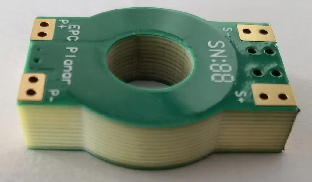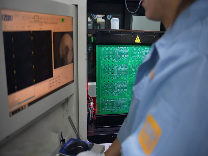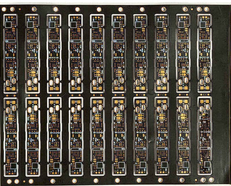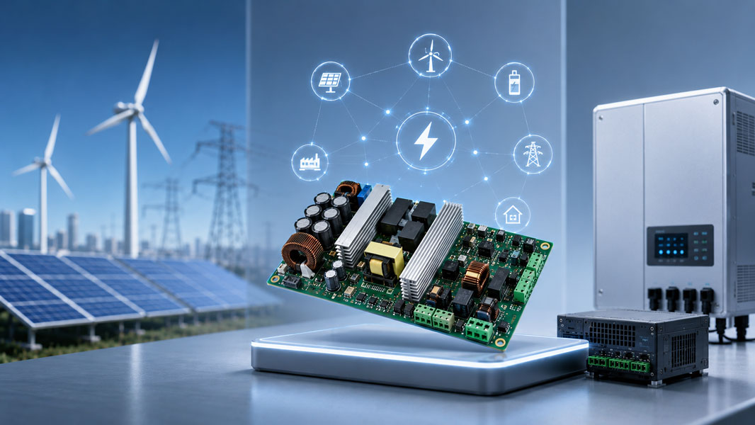
High Voltage PCB Material: Selection Guide for 2026 Why Material Choice Defines a High Voltage PCB A high voltage PCB works in circuits that carry 300, 600, 1000 volts or more, from electric vehicle power trains and energy storage to industrial power supplies, rail systems and medical equipment. At those…

Smart Water Meter PCB: Design, Materials and Cost Guide What Is a Smart Water Meter PCB? A smart water meter PCB is the control board inside a modern water meter that turns raw flow measurement into usable data. It reads the sensor, calculates consumption, stores history, drives a display and…
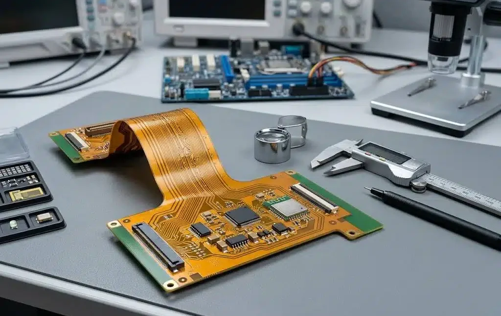
Flex PCB Outline: Design Rules, Cutting Methods and Cost What Is a Flex PCB Outline? The flex PCB outline is the mechanical profile that defines the final shape of a flexible circuit: the outer contour, internal windows, slots, mounting and tooling holes, connector areas, stiffener locations and the rounded corners…
PCB Size: Standards, Thickness, Tolerances and Cost Guide What PCB Size Really Covers PCB size is more than the length and width printed on a drawing. It includes every mechanical dimension that determines whether a board can be fabricated, assembled and installed: overall outline, board thickness, copper weight, drilled hole…
ABF PCB Substrate: 20-Layer Structure, Materials and Cost Guide What Is an ABF PCB Substrate? An ABF PCB substrate is a high density IC package substrate built with Ajinomoto Build-up Film, the ABF dielectric that enables the finest line widths and smallest laser vias in advanced semiconductor packaging. The substrate…
PCB Solder Mask Touch-Up: The Complete Repair Guide What Is PCB Solder Mask Touch-Up? PCB solder mask touch-up, sometimes called solder mask repair or spot solder mask application, is the process of repairing small local defects in the solder mask layer without rebuilding the whole board. During fabrication, handling, SMT…
Buried Via vs Microvia PCB: Full Comparison Guide Buried Vias and Microvias at a Glance Modern PCB design keeps packing more function into less space, and the wiring between layers is where the fight is won. Two advanced interconnection techniques do most of the work: buried vias, which connect inner…
Laser-Cut vs Electroformed PCB Stencil: Which Is Better? What Is a PCB Stencil? A PCB stencil, also called an SMT stencil or solder paste stencil, is the tool that decides how much solder paste lands on every pad of a board. The stencil is normally stainless steel or nickel with…
Semiconductor Test Burn-in Board: The Complete Guide What Is a Semiconductor Test Burn-in Board? A semiconductor test burn-in board is a high reliability PCB that sits between a device under test and the burn-in oven or automatic test equipment used to qualify chips. Each board carries a number of test…
Dog Bone vs Via-in-Pad PCB: Which BGA Fan-Out Design Is Better? What Are Dog Bone and Via-in-Pad Fan-Out? Every PCB that carries a fine-pitch BGA package faces the same question at the layout stage: how do we break the hundreds of solder balls out to the inner layers and the…