KingdaKingdaKingda

Call Us 24/7

+86-181-2376-9076

Send Us Mail

sales@gopcba.com

Our Location

Baoan District, Shenzhen, China

Language

  • enEnglish
    • fr France
    • itItalian
Kingda
  • Home
  • PCB Assembly
    • Prototype PCB Assembly
    • Turnkey PCB Assembly
    • Low Volume PCB Assembly
    • High Volume PCB Assembly
    • SMT PCB Assembly
    • Through-Hole PCB Assembly
    • Mixed Technology PCB Assembly
    • Flex PCB Assembly
  • Services
    • PCB Design/Layout
    • PCB Manufacturing
    • Rapid PCBA Prototyping
    • Components Procurement
    • Conformal Coating
    • PCBA Testing
    • Box Build Assembly
    • Wire & Cable Harness Assembly
  • Industry Solutions
    • Medical PCBA
    • Telecommunications PCBA
    • Energy PCBA
    • Industrial PCBA
    • Artificial Intelligence PCBA
    • IOT PCBA
  • Resources
    • PCB Capabilities
    • PCBA Capabilities
    • FAQ
    • Blog
  • About Us
    • About Us
    • Why Us
    • Quality Management
  • Contact Us
Get A Quote
1-5

Dry Film: 5 Rules for Lamination Control

  • By Frank guo
  • 2026年 9月 13日
  • PCB Assembly
  • No Comments
Dry Film: 5 Rules for Lamination Control A dry film is a photosensitive resist supplied as a thin layer on a carrier sheet, and it is laminated onto the copper surface before imaging. Compared with a liquid resist it gives a uniform thickness across the panel, which is why it…
Continue Reading
Robotic arm PCBA

Tented Via: 5 Rules for Mask Coverage

  • By Frank guo
  • 2026年 9月 13日
  • PCB Assembly
  • No Comments
Tented Via: 5 Rules for Mask Coverage A tented via is a via whose opening is covered by solder mask, so the hole and its annular ring are sealed under the coating instead of being left open. The purpose is simple. An open via next to a pad can wick…
Continue Reading
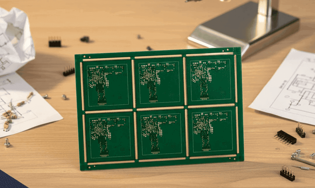
PCB

Step Board: 5 Rules for Cavity Depth Control

  • By Frank guo
  • 2026年 9月 13日
  • PCB Assembly
  • No Comments
Step Board: 5 Rules for Cavity Depth Control A step board is a printed circuit board with a pocket milled into it so that a tall component can sit below the surface of the panel. The pocket, usually called a cavity, is created by controlled routing depth, and it lets…
Continue Reading
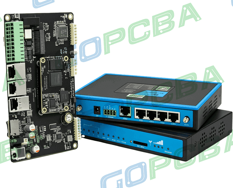
Industrial communication gateway PCBA

Stacked Via: 5 Rules for HDI Reliability

  • By Frank guo
  • 2026年 9月 13日
  • PCB Assembly
  • No Comments
Stacked Via: 5 Rules for HDI Reliability A stacked via is a microvia placed directly on top of another microvia, so the connection passes through two or more HDI layers without a landing pad between them. The arrangement saves the space that an offset or staggered build would need, which…
Continue Reading
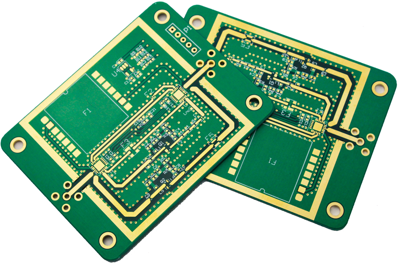
PCB Manufacturing

Solder Fountain: 5 Rules for Selective Soldering

  • By Frank guo
  • 2026年 9月 13日
  • PCB Assembly
  • No Comments
Solder Fountain: 5 Rules for Selective Soldering A solder fountain is the small, localised wave that a selective soldering machine raises under a single through hole component, and its height decides how much of the barrel the alloy touches. Setting that height is more delicate than it looks, because the…
Continue Reading
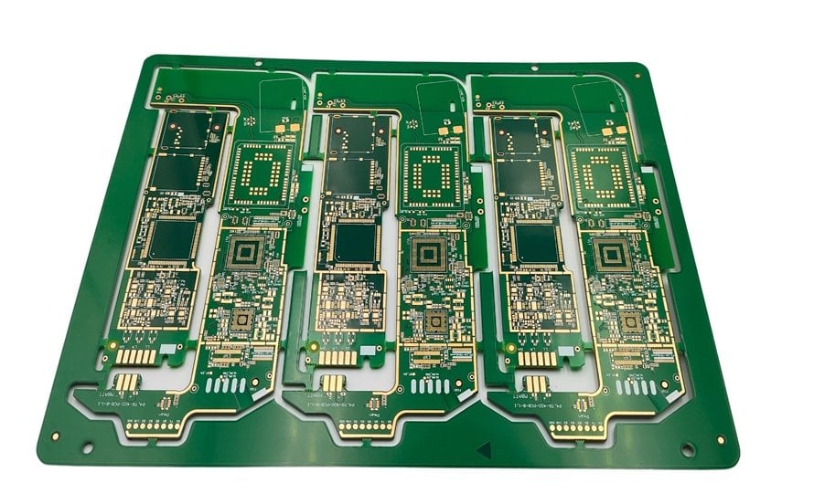
HDI PCB Design Guide

Nanocoating: 5 Rules for Stencil Paste Release

  • By Frank guo
  • 2026年 9月 13日
  • PCB Assembly
  • No Comments
Nanocoating: 5 Rules for Stencil Paste Release Stencil nanocoating is a thin film applied to the aperture walls of a laser cut stencil so that solder paste releases cleanly rather than smearing down the side of the opening. On a stainless steel stencil that has no coating, the striated edge…
Continue Reading
Quick Turn PCB Fabrication

Outgassing: 5 Causes in Lamination and Assembly

  • By Frank guo
  • 2026年 9月 13日
  • PCB Assembly
  • No Comments
Outgassing: 5 Causes in Lamination and Assembly Outgassing is the release of trapped gas from inside a board when it is heated. The gas comes from moisture absorbed by the laminate, from volatiles left in the resin and from air trapped in a via or under a plane, and it…
Continue Reading
ptt_gallery

Entry Material: 5 Rules for Hole Quality

  • By Frank guo
  • 2026年 9月 13日
  • PCB Assembly
  • No Comments
Entry Material: 5 Rules for Hole Quality Entry material is the sheet that sits on top of the panel when it is drilled. It looks like a consumable detail, and it decides a surprising amount about the quality of the hole: it cushions the drill as it enters, it holds…
Continue Reading
16

Solder Skip: 5 Causes on a Wave Solder Line

  • By Frank guo
  • 2026年 9月 13日
  • PCB Assembly
  • No Comments
Solder Skip: 5 Causes on a Wave Solder Line A solder skip is a pad or a lead that passes over the wave without being soldered, leaving the metal bright and bare. It is different from a cold joint, because no alloy was ever applied, and different from a missing…
Continue Reading
PCB Drilling

Metal Squeegee: 5 Rules for a Clean Wipe

  • By Frank guo
  • 2026年 9月 13日
  • PCB Assembly
  • No Comments
Metal Squeegee: 5 Rules for a Clean Wipe A metal squeegee is the steel blade that pushes solder paste across the stencil. It is chosen because it keeps a sharp edge for a very long time, which makes the print repeatable from the first board of a campaign to the…
Continue Reading
1 … 60 61 62 … 591

Search Posts

Categories

  • Electronic Materials
  • Electronical Engineering
  • Industrial Control
  • PCB Assembly
  • PCB Design
  • PCB Manufacturing

Recent Posts

Surface Mount Technology (SMT): Process, Components, Design Guidelines & PCB Assembly

Surface Mount Technology (SMT): Process, Components, Design Guidelines & PCB Assembly

Zane Zhang - 2026年 10月 2日
Cheap PCB Costs: PCB Design, PCB Manufacturing & SMT vs TH Guide

Cheap PCB Costs: PCB Design, PCB Manufacturing & SMT vs TH Guide

Jelly - 2026年 9月 30日
Cheap PCB Costs: PCB Design, PCB Manufacturing & SMT vs TH Guide

Cheap PCB Costs: PCB Design, PCB Manufacturing & SMT vs TH Guide

Jelly - 2026年 9月 30日

Tags

AOI inspection automotive electronics automotive PCBA quality automotive standards box build assembly component mounting component procurement component supplier conformal coating defect prevention DFM checks DFM review e-bom management electronic component shortage electronic manufacturing services electronic manufacturing standards Electronic Materials electronics design best practice electronics manufacturing capacity electronics sourcing high volume production industrial electronics insertion mount manufacturability review mass production quality mixed technology PCB PCBA inspection PCBA prototype PCBA turnkey PCBA volume pricing PCB Design PCB layout rules PCB Manufacturing PCB sourcing power electronics PCB printed circuit board prototype quick turn PCB reflow soldering SMT assembly quality SMT production solder paste inspection solder paste printing surface mount technology vehicle electronics wave soldering
GOPCBA-logo

As a professional China PCB assembly manufacturer, we provide a full range of electronic manufacturing services from PCB fabrication, PCBA to OEM/ODM, including PCB design, PCB layout, rapid PCBA prototyping, components procurement, SMT/ THT assembly, china pcb assembly, china pcb prototype, PCBA testing and box build assembly.

Linkedin Facebook-f X-twitter Youtube Instagram

PCB ASSEMBLY

  • Prototype PCB Assembly
  • Low Volume PCB Assembly
  • High Volume PCB Assembly
  • Turnkey PCB Assembly
  • SMT PCB Assembly
  • Through-Hole PCB Assembly
  • Mixed Technology PCB Assembly
  • Flex PCB Assembly

OUR SERVICES

  • PCB Design/Layout
  • PCB Manufacturing
  • Rapid PCBA Prototyping
  • Components Procurement
  • Conformal Coating
  • PCBA Testing
  • Box Build Assembly
  • Wire & Cable Harness Assembly

TECHNICAL SUPPORT

  • About Us
  • Quality Management
  • Artificial Intelligence PCBA
  • Industrial PCBA
  • IOT PCBA
  • Medical PCBA
  • Energy PCBA
  • Telecommunications PCBA

Copyright © 2026. Shenzhen Kingda Electronics Co., LTD  All rights reserved. 

  • Sitemap
  • Terms of Service
  • Privacy Policy
Zmdi Zmdi-email Phone-square Whatsapp Weixin
x

ABOUT US

Progressively maintain extensive infomediaries via extensible nich. Capitalize on low hanging fruit. a ballpark value added is activity to beta test. Override the digital divide with additional click throughs from fruit.

LOCATIONS

map

New York Office

+07 554 332 322
contact@example.com
office@example.com
37 San Fairport, NY 14450, New York City
All Locations

FOLLOW US