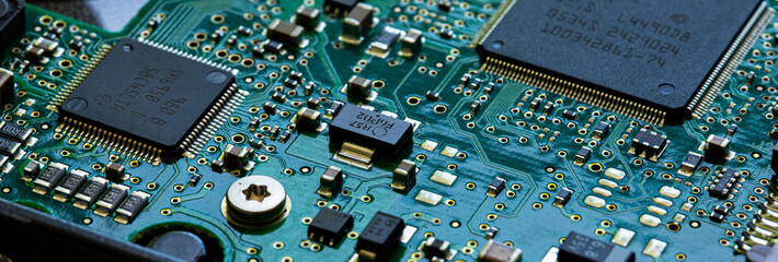

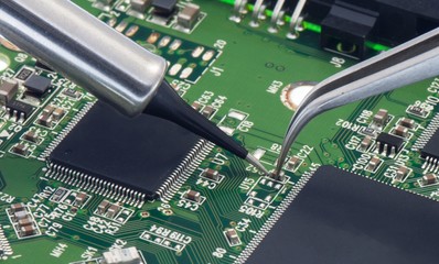
Inverter PCB Manufacturer for Power and Solar Designs An inverter board carries two very different jobs on one surface. It switches large currents through power devices, and it also measures, controls, and protects those same devices. A capable inverter PCB manufacturer must plan for both duties from the first stackup…
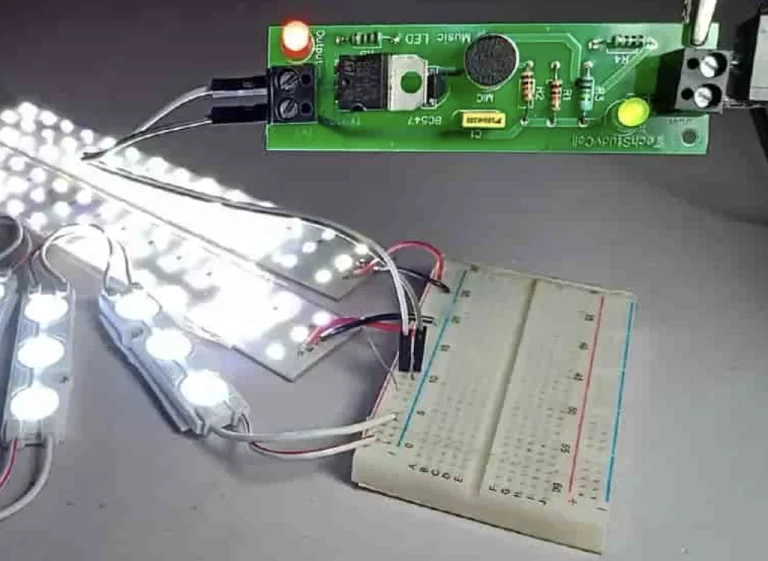
LED PCB Manufacturing: Thermal Design and Assembly An LED board fails for reasons that rarely appear on the drawing. Heat builds under a dense array, current spreads unevenly, or a solder joint opens after thermal cycling. The board itself must carry heat away, hold tight placement, and keep current stable…
Power PCB Manufacturing for High-Current Designs Power boards fail for reasons that rarely appear on a quotation. Copper weight, thermal paths, via structure and material grade decide whether a design survives years of load cycling. Buyers often compare suppliers on price per square meter and miss the process controls that…
Embedded PCB Manufacturing: Component Integration Guide Embedded PCB technology places selected components inside the board instead of on its outer surfaces. This shift changes how a design is planned, built, and inspected. It also changes what a buyer should ask for before approving a quotation. The sections below explain the…
IC Substrate PCB Manufacturing Guide for Advanced Packaging An IC substrate sits between a semiconductor die and the system board. It carries fine-pitch signals, delivers power, and supports the package mechanically. Conventional PCB processes rarely reach the routing density these packages need. This guide explains how substrate fabrication works, where…
6-Layer PCB Fabrication: Stackup and Process Control A six-layer board adds two internal copper layers to a standard four-layer build. That sounds simple, but the extra layers change how signals return, how power spreads, and how the laminate behaves during pressing. Most failures on these boards trace back to decisions…
4 Layer PCB Manufacturer: Stackup and Fabrication Control A four-layer board carries two outer signal layers and two inner layers for power, ground, or routing. The extra copper buys routing room, a steady reference plane, and better power delivery than a two-layer design. It also adds process steps that a…
Single-Sided PCB Manufacturing: A Buyer’s Process Guide A single-sided board carries one copper layer, so it suits circuits that route on one plane. That simplicity drives the cost, the lead time and the process choices behind every order. This guide walks through the structure, the fabrication steps and the checks…
Quick Turn PCB Manufacturing for Fast Prototypes Conventional PCB schedules can stall an active development program. Quick turn PCB manufacturing compresses the time between a finished design and working boards in hand. Engineers then test, find problems, and revise before committing to volume. A dependable quick turn service rests on…
Low Loss PCB Manufacturing for High-Speed Designs A low loss PCB keeps signal energy in the trace instead of losing it to the dielectric and copper. At high frequency, that difference decides whether a link closes its loss budget. The board itself is only part of the story. Material choice,…