Inverter PCB Manufacturer for Reliable Power Conversion
A reliable inverter PCB is the foundation of modern power conversion equipment. It supports the control, switching, protection, monitoring, and power management functions required to convert DC power into stable AC output.
At Gopcba, we provide customized PCB fabrication and assembly solutions for inverter applications, including renewable energy systems, industrial power equipment, automotive electronics, portable power systems, and other power-conversion products.
Our manufacturing capabilities support conventional multilayer boards as well as high-TG, heavy-copper, metal-core, HDI, high-frequency, and controlled-impedance PCB technologies. PCB Manufacturing
What Is an Inverter PCB?

An inverter PCB is a printed circuit board designed for electronic inverter systems that convert direct current (DC) into alternating current (AC). Depending on the application, the DC source may come from batteries, photovoltaic panels, fuel cells, energy-storage systems, vehicle electrical systems, or other DC power sources.
A typical inverter system may include:
- Power semiconductor switches
- Gate-driver circuits
- Microcontrollers or digital control processors
- DC/DC conversion circuits
- DC-link capacitors
- Output filtering circuits
- Voltage and current sensing circuits
- Protection circuits
- Communication interfaces
- Thermal-management components
The PCB must provide reliable electrical connections while managing high current, switching noise, heat, insulation requirements, and electromagnetic interference.
For complete electronic production, PCB fabrication can also be combined with PCB Assembly services covering SMT, through-hole, mixed-technology, inspection, and testing.
Applications of Inverter PCBs
The demand for power PCB solutions continues to increase as electrification, renewable energy, energy storage, and industrial automation expand.
Common applications include:
Solar and Renewable Energy
A solar inverter PCB is used in photovoltaic power systems to control the conversion of DC electricity generated by solar panels into usable AC electricity.
Typical applications include:
- Residential solar inverters
- Commercial photovoltaic systems
- Utility-scale solar equipment
- Energy-storage systems
- Hybrid solar inverters
- Microinverters
- Battery energy-storage systems
Automotive and Electric Vehicles
Automotive inverter electronics are used in electric and hybrid vehicles for motor control and power conversion.
The PCB may need to withstand:
- High current
- Rapid switching
- Vibration
- Temperature cycling
- Electromagnetic interference
- High-voltage operating conditions
Industrial Equipment
Industrial motor drives, automation equipment, pumps, compressors, welding equipment, and power supplies can all require specialized inverter PCB manufacturing solutions.
Portable Power Equipment
Compact inverter systems are commonly used in portable power stations, emergency power equipment, outdoor power systems, and mobile electrical equipment.
Key Materials for Inverter PCB Manufacturing
Material selection directly affects electrical insulation, thermal performance, mechanical reliability, and operating temperature.
Depending on the design, Gopcba can support different PCB material technologies.
High-TG FR-4
High-TG FR-4 is widely used in power electronics where higher thermal resistance and dimensional stability are required.
It is suitable for many industrial and commercial inverter designs where cost, reliability, and manufacturability must be balanced.
Heavy Copper PCB
High-current inverter circuits can generate significant electrical and thermal loads. Heavy copper construction increases current-carrying capability and can improve heat distribution.
For demanding power applications, heavy copper technology can therefore be an important power PCB solution.
Metal Core PCB
Metal-core PCBs provide an efficient thermal path for applications with high heat generation.
They are particularly useful when heat dissipation is an important design requirement and the PCB must transfer heat away from power components.
High-Frequency Materials
High-frequency materials can be considered when an inverter design includes high-speed switching, sensitive control signals, or demanding signal-integrity requirements.
Ceramic PCB
Ceramic substrates may also be selected for specialized high-temperature or high-power applications where thermal conductivity and electrical insulation are critical.
The optimum material should always be selected according to voltage, current, switching frequency, operating temperature, mechanical requirements, thermal design, and expected service life.
Important Design Considerations for Inverter PCBs
A successful inverter PCB manufacturer must consider much more than basic PCB fabrication. Power electronics require careful coordination between electrical design, thermal management, component selection, PCB layout, manufacturing processes, and testing.
Selecting the Power Semiconductor
The switching device is one of the most important decisions in inverter design.
Common technologies include:
- Silicon MOSFETs
- IGBTs
- Silicon Carbide (SiC) devices
- Gallium Nitride (GaN) devices
The correct choice depends on switching frequency, voltage, current, efficiency, thermal performance, cost, and application requirements.
SiC and GaN devices can provide advantages in specific high-efficiency and high-frequency applications, while silicon MOSFETs and IGBTs remain widely used across many inverter architectures.
Working Voltage and Electrical Protection
The PCB must be designed according to the maximum operating voltage, transient voltage, switching behavior, insulation requirements, and protection strategy of the complete inverter system.
Important protection functions may include:
- Overvoltage protection
- Overcurrent protection
- Short-circuit protection
- Overtemperature protection
- Undervoltage lockout
- Desaturation protection
- Gate-drive protection
- Surge protection
Proper creepage and clearance distances are also essential for high-voltage designs.
PCB Layout for Inverter Applications
PCB layout has a direct impact on inverter efficiency, electromagnetic compatibility, thermal performance, and reliability.
The high-current switching loop should be designed with short and controlled current paths. Excessive loop area can increase parasitic inductance and switching transients.
Important layout principles include:
- Keep high-current paths short
- Minimize unnecessary vias
- Reduce switching-loop area
- Separate high-voltage and low-voltage circuits
- Separate power and sensitive control circuits
- Keep gate-driver traces short
- Place decoupling capacitors close to switching devices
- Provide appropriate thermal paths
- Maintain sufficient creepage and clearance
- Use suitable ground and return-current structures
For complex designs, professional PCB Design and Layout support can help evaluate stackup, impedance, manufacturability, EMI/EMC, and thermal considerations before production.
Thermal Management
Power semiconductor devices can generate substantial heat during operation.
A reliable inverter PCB should therefore provide an appropriate thermal path from the power components to the PCB, heatsink, chassis, or other cooling structure.
Thermal-management techniques may include:
- Heavy copper
- Thermal vias
- Copper planes
- Metal-core substrates
- External heatsinks
- Thermal interface materials
- Improved airflow
- Optimized component placement
Temperature-sensitive components should be positioned away from high-temperature power devices whenever possible.
Signal Isolation and Noise Control
Inverter circuits typically combine high-power switching with low-level control and sensing signals. Poor PCB layout can allow switching noise to interfere with control circuits.
Designers should consider:
- Physical separation between power and control sections
- Appropriate grounding strategies
- Differential sensing
- Shielding where required
- Short gate-drive connections
- Proper decoupling
- Controlled return-current paths
- EMI filtering
These measures can improve system stability and reduce unwanted electromagnetic interference.
Solar Inverter PCB Design
A solar inverter PCB has additional requirements because photovoltaic systems are often exposed to outdoor operating conditions and variable input power.
The design may need to accommodate:
- Wide DC input ranges
- Variable photovoltaic output
- High conversion efficiency
- DC isolation
- Grid synchronization
- MPPT control
- Surge protection
- Thermal cycling
- Long operating periods
- Environmental exposure
Depending on the architecture, solar inverter PCBs may be used in string inverters, central inverters, microinverters, hybrid inverters, and energy-storage systems.
For higher reliability, the PCB material, copper thickness, component selection, insulation system, coating, and thermal design should be evaluated together rather than independently.
Inverter PCB Types
Different inverter architectures require different PCB structures.
Single-Phase Inverter PCB
Single-phase inverter boards are commonly used in residential appliances, portable power equipment, small solar systems, and other low-to-medium power applications.
Three-Phase Inverter PCB
Three-phase inverter systems are widely used in industrial motors, commercial power systems, electric vehicles, renewable-energy equipment, and other higher-power applications.
High-Power Inverter PCB
High-power systems typically require stronger current-carrying capability, improved thermal management, higher-voltage insulation, and more robust power-device connections.
Heavy copper and specialized materials may be considered depending on the electrical requirements.
Multilayer Inverter PCB
Multilayer construction can provide additional routing space, improved power distribution, controlled impedance, better signal isolation, and more compact system integration.
Gopcba supports a broad range of PCB structures and production technologies through its PCB Capabilities for prototype and production applications.
Inverter PCB Manufacturing Process
Professional inverter PCB manufacturing requires consistent process control from engineering review through final inspection.
A typical manufacturing workflow includes:
1. Engineering Review
The manufacturing team reviews Gerber files, drawings, stackup requirements, material specifications, copper thickness, tolerances, and special processing requirements.
2. DFM Analysis
Design-for-manufacturing analysis identifies potential fabrication problems before production.
Typical checks include:
- Minimum trace width and spacing
- Annular ring
- Drill sizes
- Copper distribution
- Solder-mask clearance
- Via structures
- Layer registration
- Thermal requirements
3. PCB Fabrication
The PCB is manufactured through processes such as imaging, etching, lamination, drilling, copper plating, solder-mask application, surface finishing, and electrical testing.
For complex products, manufacturing may include multilayer, HDI, blind/buried vias, heavy copper, or other specialized structures.
4. PCB Assembly
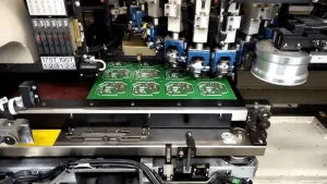
After PCB fabrication, components can be assembled using SMT, through-hole, or mixed-technology processes.
For projects requiring a complete manufacturing solution, Turnkey PCB Assembly can integrate PCB fabrication, component sourcing, assembly, inspection, and testing.
5. Inspection and Testing
Quality control may include:
- AOI
- X-ray inspection
- Electrical testing
- Visual inspection
- Solder-joint inspection
- Functional testing
- Component verification
The exact inspection strategy depends on the PCB structure and application requirements.
PCB Assembly for Inverter Applications
PCB fabrication is only one part of the production process. Inverter products often require reliable assembly of power semiconductors, connectors, capacitors, sensors, controllers, and other components.
A complete assembly solution can include:
- SMT assembly
- THT assembly
- Mixed-technology assembly
- BGA assembly
- Component sourcing
- Programming
- Electrical testing
- Functional testing
- Conformal coating
- Final product assembly
For products combining surface-mount and through-hole components, Mixed Technology PCB Assembly can provide an integrated production process.
Quality Requirements for Inverter PCBs
Quality requirements should be defined according to the electrical and environmental demands of the final product.
Important parameters may include:
- Dimensional accuracy
- Layer-to-layer registration
- Copper thickness
- Dielectric thickness
- Trace width and spacing
- Hole diameter
- Via reliability
- Surface finish
- Insulation resistance
- Electrical continuity
- Thermal performance
- Solderability
- Mechanical reliability
For high-reliability applications, manufacturing inspection and testing should be established according to the product’s industry, operating environment, and applicable standards.
Why Choose Gopcba for Inverter PCB Manufacturing?
Gopcba provides integrated PCB and PCBA manufacturing services for customers developing power electronics, industrial equipment, energy systems, automotive electronics, and other demanding applications.
The manufacturing platform supports PCB fabrication, component procurement, SMT assembly, through-hole assembly, testing, and finished-product integration.
Key advantages include:
- Custom PCB manufacturing
- Multilayer PCB production
- HDI and high-density PCB technology
- High-TG PCB
- Heavy copper PCB
- High-frequency PCB
- Metal-core PCB
- Controlled-impedance PCB
- PCB design and engineering support
- SMT and through-hole assembly
- Prototype and production manufacturing
- Component sourcing
- PCBA testing
For projects that require smaller production quantities or an accelerated development cycle, Low Volume PCB Assembly provides a practical path from prototype to production.
Prototype to Mass Production
Inverter products often go through several development stages before entering volume production.
A reliable manufacturing partner should be able to support:
Engineering Review → Prototype → Testing → Design Optimization → Low-Volume Production → Mass Production
This approach allows engineers to identify electrical, thermal, assembly, and manufacturing issues before committing to large production quantities.
Gopcba supports prototype, low-volume, and mass-production requirements, helping customers maintain manufacturing continuity as their products move through different development stages.
How to Choose an Inverter PCB Manufacturer
When selecting an inverter PCB manufacturer, evaluate the supplier according to both technical capability and production reliability.
Important factors include:
Manufacturing Capability
Confirm whether the supplier can manufacture the required layer count, copper thickness, material system, via structure, surface finish, and board dimensions.
Power Electronics Experience
A manufacturer experienced with power electronics should understand the importance of heavy copper, thermal management, insulation distances, power distribution, and high-current routing.
Engineering Support
DFM review and engineering communication can identify potential manufacturing problems before production begins.
Assembly Capability
If PCB fabrication and assembly are handled by the same supplier, communication and production coordination can become more efficient.
Quality Control
Ask about AOI, X-ray inspection, electrical testing, process control, traceability, and final inspection.
Production Flexibility
The supplier should be capable of supporting prototypes, low-volume orders, and volume production without requiring a complete change of manufacturing partner.
Frequently Asked Questions
What is an inverter PCB?
An inverter PCB is a printed circuit board used inside an inverter system to control power conversion, switching, sensing, protection, filtering, and communication functions.
What is the difference between an inverter PCB and a standard PCB?
An inverter PCB often operates under higher current, voltage, temperature, and switching stress than a conventional control board. It therefore requires more careful consideration of copper thickness, thermal management, electrical insulation, layout, and component placement.
What materials are used for inverter PCBs?
Common choices include standard and high-TG FR-4, heavy copper, metal-core materials, high-frequency laminates, and ceramic substrates. The appropriate material depends on the electrical and thermal requirements.
What is a solar inverter PCB?
A solar inverter PCB is designed for photovoltaic inverter systems. It supports functions such as DC-to-AC conversion, MPPT control, monitoring, protection, and grid or load interfacing.
Can you manufacture custom inverter PCBs?
Yes. Custom PCB manufacturing can be based on customer Gerber files, PCB drawings, stackup requirements, material specifications, component information, and production quantities.
Can inverter PCB manufacturing include PCB assembly?
Yes. PCB fabrication can be combined with SMT, THT, mixed-technology assembly, component sourcing, inspection, testing, and other PCBA services.
What should be considered when designing an inverter PCB?
The main considerations include operating voltage, current, switching frequency, power-device selection, thermal management, creepage and clearance, PCB material, copper thickness, EMI/EMC, grounding, signal isolation, and manufacturing capability.
How can I get a quotation for an inverter PCB?
Provide the PCB Gerber files, BOM, assembly drawings, PCB specifications, required quantity, and any special technical requirements. The manufacturing team can then evaluate the design and provide a suitable production solution.