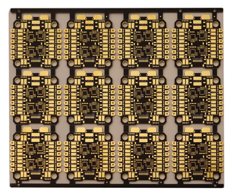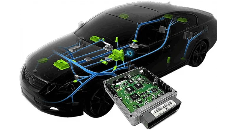
PCB Squeegee Pressure and Angle: Pushing the Paste Through Electronics manufacturing has become a discipline of small details. Solder paste volumes, placement accuracy, temperature profiles and inspection limits all add up to the final result. This guide looks at PCB squeegee pressure and angle from the perspective of a PCBA…
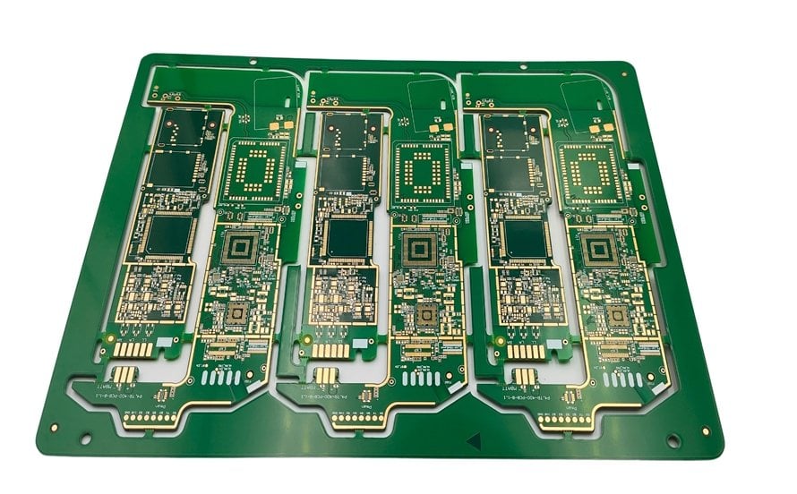
PCB Nozzle Selection for Placement: The Right Tip for the Part Modern electronics depend on boards that are assembled correctly the first time. Every product – a phone, a charger, a medical instrument or an industrial controller – relies on thousands of solder joints that must conduct current for years.…
PCB Solder Paste Inspection After Print: Before the Parts Arrive Buyers and engineers often focus on the finished product and forget the production line behind it. In practice, most field failures can be traced back to process decisions made during assembly. Understanding PCB solder paste inspection after print gives you…
PCB Placement Force on A Fine Pitch Part: How Hard the Nozzle Pushes Buyers and engineers often focus on the finished product and forget the production line behind it. In practice, most field failures can be traced back to process decisions made during assembly. Understanding PCB placement force on a…
Transportation IoT Board: Design Guide for Vehicle Systems An IoT board that is installed in a transport system has a harder life than one that sits on a desk. It is powered from a vehicle supply that is never clean, it is mounted where it is shaken, it must operate…
Machine Vision PCB: Sensor Interface and Power Noise A machine vision board exists to move image data from a sensor to a processor without corrupting it. That sounds simple, and it becomes difficult because the data rate is high, the sensor is sensitive to its supply and its clock, and…
Press-Fit Connector PCB: Hole Design and Assembly Requirements A press-fit connector is attached by pushing pins into plated through holes instead of soldering them. The joint relies on mechanical interference: the pin compresses against the barrel wall and creates a gas-tight contact that carries current and holds the connector in…
Heavy Copper PCB Prototyping: Design Rules and Process Control Heavy copper PCB work starts where conventional boards stop: above about 3 oz of finished copper per layer. The thicker metal carries far more current, spreads heat under power devices and survives mechanical stress better, but it also changes every process…
IC Package Substrate: Structure, Materials and Build-Up Layers An IC package substrate is the board that carries a bare die and connects its micrometre scale bumps to millimetre scale board pads. It redistributes power, ground and high speed signals, manages heat, and protects the device during assembly. As packages have…
PCB Via Hole Guide: Types, Sizes and Aspect Ratio A via hole is the smallest feature that decides whether a board can be built at all. Diameter, depth, pad size and plating thickness are linked, and pushing one of them past the process window turns a routine multilayer board into…