PCB Copper Roughness and Loss: The Bumps Under the Skin Electronics manufacturing has become a discipline of small details. Solder paste volumes, placement accuracy, temperature profiles and inspection limits all add up to the final result. This guide looks at PCB copper roughness and loss from the perspective of a…
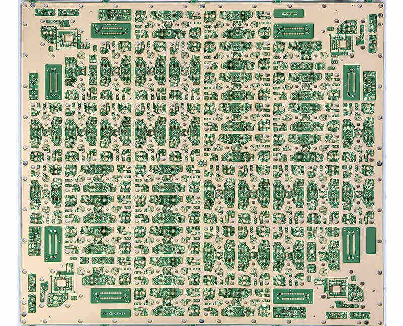
PCB Panel Utilisation: Getting More Boards From a Sheet Buyers and engineers often focus on the finished product and forget the production line behind it. In practice, most field failures can be traced back to process decisions made during assembly. Understanding PCB panel utilisation gives you a practical advantage when…
Drone PCB Cost: What Drives the Price of Flight Controller Boards Drone PCB cost is shaped by constraints that have nothing to do with the circuit: weight, vibration, thermal extremes and a very small available volume. A flight controller board is usually 30 to 50 millimetres square and carries a…
PCB Plating Thickness in A Barrel: How Much Copper Is Enough Electronics manufacturing has become a discipline of small details. Solder paste volumes, placement accuracy, temperature profiles and inspection limits all add up to the final result. This guide looks at PCB plating thickness in a barrel from the perspective…
Video Recorder PCB: Design for High Speed Video Capture A video recorder board is a small system that happens to be shaped like a circuit board. It has to capture a high bandwidth data stream from an image sensor or a video decoder, process it, buffer it, write it to…
PCB Differential Pair Skew Matching: Keeping the Two Halves Together Electronics manufacturing has become a discipline of small details. Solder paste volumes, placement accuracy, temperature profiles and inspection limits all add up to the final result. This guide looks at PCB differential pair skew matching from the perspective of a…
Laptop PCB Design: Layer Count, Space and Thermal Limits A laptop main board is one of the densest products in consumer electronics. It carries a processor with a thousand or more connections, a memory interface running at multi-gigabit rates, several high-speed serial links to the display and the storage, a…
PCB Traces: Structure, Materials and Design Rules A trace is a copper conductor manufactured by etching away everything around it, and its shape is the whole of its electrical behaviour. Width, thickness, length and the distance to its reference plane determine resistance, inductance, impedance and how much it disturbs its…
PCB Loss Tangent at High Frequency: Where the Signal Turns Into Heat Modern electronics depend on boards that are assembled correctly the first time. Every product – a phone, a charger, a medical instrument or an industrial controller – relies on thousands of solder joints that must conduct current for…
WiFi PCB and Bluetooth PCB: What Changes in the Layout Wireless products look similar on the schematic but behave very differently on the board. A WiFi PCB works in a wide channel with high throughput and strict emission limits, while a Bluetooth PCB works in a narrow band at much…