Custom PCB Cost: The Technical Factors Behind the Price Custom PCB cost is not a single number produced by a price list. It is the sum of material, process steps, tooling, inspection and volume, and the weight of each item changes with the design. Two boards of identical size can…
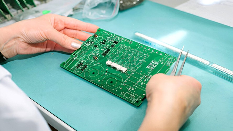
Double-Sided PCB Manufacturing: Process and Design Rules A double-sided PCB carries copper on both surfaces and connects the two with plated through-holes. It is the workhorse of electronic manufacturing: more capable than a single-sided board, far less expensive than a multilayer stack, and adequate for the majority of products that…
Castellated Hole FR4 PCB: What Designers Need to Know A castellated hole is a plated through hole that is drilled on the edge of a panel and then cut in half during routing, leaving a plated semicircular notch along the board outline. The result looks minor but changes everything about…
Aluminum Nitride PCB: Thermal Performance and When It Pays Most thermal problems on a circuit board are solved with copper, vias and a heat sink. Some of them cannot be. When a device dissipates hundreds of watts in a few square centimetres and must remain electrically isolated from its heat…
Stacked Microvias: Structure, Process and Reliability When a board runs out of room, the vias are usually the first thing to blame. A through-hole occupies every layer it passes through, so a dense design ends up paying for routing area it cannot use. Stacked microvias solve that by making the…
Automotive PCB Requirements: Materials, Layers and Qualification Automotive electronics is the most demanding mainstream application for printed circuit boards. A board that fails in a phone is an inconvenience, while the same failure in a braking or steering system is a safety event. That difference explains why automotive PCB requirements…
What Is a Backplane PCB? Design and Applications A backplane is the board that holds a system together. It carries no display, no processor and often very few components, yet it determines the data rate the system can reach, the number of cards it can hold and how reliably it…
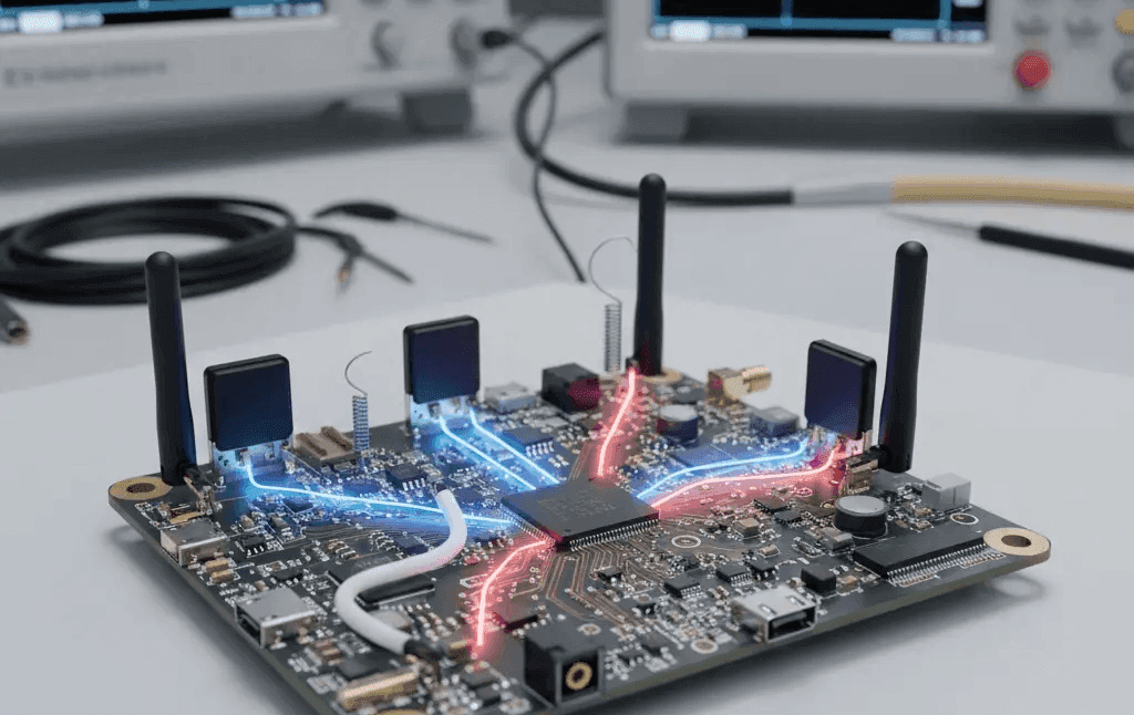
PCBA Antenna Design: Types and Layout Rules An antenna that is designed into the board rather than screwed onto the enclosure has obvious commercial advantages: lower cost, smaller size, no assembly step and no connector to work loose. It also turns the layout into part of the radio, because the…
PCB Etching: Chemistry, Etch Factor and Width Tolerance Etching is the step that turns a copper-clad panel into a circuit. A resist pattern is printed or laminated onto the copper, the panel passes through a chemical bath that dissolves the metal not protected by the resist, and what remains is…
Switching Power Supply PCB: Design Guide and Best Practices Switch mode conversion has displaced linear regulation in almost every application above a few watts, because the efficiency gain translates directly into smaller heatsinks, smaller enclosures and longer run time from a battery. The price of that efficiency is a far…