Switching Power Supply PCB: Design Guide and Best Practices
Switch mode conversion has displaced linear regulation in almost every application above a few watts, because the efficiency gain translates directly into smaller heatsinks, smaller enclosures and longer run time from a battery. The price of that efficiency is a far more demanding layout. A switching power supply PCB carries large pulsed currents, fast voltage edges and heat within the same small area, and the layout decides whether the design meets its efficiency target or radiates noise across the whole product. This guide walks through the decisions that matter, from topology selection through to the test bench.
Converter Topologies and When to Use Them
Topology follows the relationship between input and output rather than personal preference. A buck converter steps a higher input down to a lower rail and remains the workhorse of point-of-load regulation because it is simple, efficient and well understood. A boost converter does the opposite, raising a low battery voltage to a higher bus, and it is the usual choice for driving LED strings and for power factor correction stages. A buck-boost or single-ended inductive converter covers the awkward case where the input may sit above or below the output, such as a battery rail that starts at 4.2 V and discharges to 3.0 V while the load needs a fixed 3.3 V.
Isolated topologies appear once safety separation is required or once the power level rises. The flyback converter dominates low-power offline supplies because it uses a single switch and a coupled inductor to provide both energy transfer and isolation, at the cost of high peak currents and significant ringing. Forward, half-bridge and full-bridge converters take over at higher power, where the transformer is driven in a more symmetric manner and the stress per device falls. Choosing the wrong family is expensive to reverse later, because the magnetics, the switch ratings and the snubber network all follow from that single decision.
Choosing the Power Stage Components
The switching device sets the achievable efficiency more than any other part. Conduction loss scales with the square of the current and with the on-resistance of the device, while switching loss scales with frequency, voltage and the charge that must be moved through the gate and the output capacitance. The practical consequence is that gate charge and on-resistance have to be traded against each other. A device with very low on-resistance usually carries a large die and therefore large parasitic capacitance, which makes it a poor fit for a compact high-frequency design and an excellent fit for a low-frequency high-current one.
The inductor and the output capacitors carry the remaining burden. Core material determines the loss as a function of ripple and frequency, and saturation current must be checked against the worst-case peak rather than the average. On the output side, a combination of bulk capacitance for energy storage and small ceramic parts for high-frequency impedance keeps the ripple within specification, but only if the ceramics are placed close enough that their loop inductance does not defeat them. Rectification matters as well: a schottky diode removes the reverse recovery problem, while a synchronous rectifier removes the forward drop entirely and is now standard in anything that must be efficient.
Minimising the High Current Loop
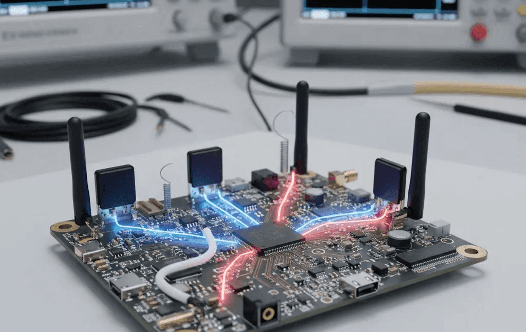
The single most important layout rule in a switching supply is to keep the loop that carries the pulsed current as small as the geometry allows. That loop is formed by the input capacitor, the switching device and the freewheeling path, and every square millimetre of it contributes inductance. Inductance in that loop produces a voltage spike at the switching node and radiates a magnetic field that will be picked up by nearby signal traces. Placing the input capacitor immediately beside the switch, connecting it with a plane or with multiple vias rather than a single trace, and keeping the return path directly underneath the outgoing path all shrink the loop without changing the schematic at all.
<img src="https://www.gopcba.com/wp-content/uploads/2024/09/tupan1.png" alt="switching power supply PCB with tight high current loop and thermal vias” />
After the switching node, the current becomes a triangle rather than a pulse, and the layout constraints relax considerably. This is why the output filter can sit further away and why the feedback network can be routed with ordinary care. The one exception is the sense path: the feedback divider should be connected to the output at the point where the regulation is actually required, using a Kelvin connection if the load current is large, because a few milliohms of trace resistance will otherwise appear as a load-dependent offset in the regulation.
Grounding Strategy
Every switching supply needs a ground plane rather than a web of traces, and it needs the plane to be continuous under the critical loop. Splitting the ground into a power ground and a signal ground and joining them at a single point is a common remedy for mixed-signal boards, but the join must be placed so that no signal return current has to detour through it. The test is to ask where the current actually flows, not where the schematic labels say it flows, and to keep the return path under its forward path for every high-frequency net.

Control circuitry deserves the same discipline. The compensation network, the current sense amplifier and the reference should be referenced to a quiet area of copper that is not shared with the switching return, and the gate drive return should be as short as possible. Our layer assignment notes describe how a stack-up is planned so that a solid reference plane is always available.
Thermal Management on a Switching Supply
Losses that look acceptable in a calculation become a temperature problem once they are concentrated in a package a few millimetres across. The switching device, the inductor winding and the output rectifier are the three usual hot spots. Copper area under the drain or the pad conducts heat into the board far better than the plastic body of the package does, so thermal vias from the exposed pad into the inner planes are the standard first step, followed by a plane that spreads the heat laterally rather than concentrating it. Our thermal management article covers the general approach and the way the numbers are estimated before anything is built.
Derating assumptions deserve scrutiny as well. A supply that runs at its rated output in still air inside a sealed enclosure sees a very different ambient from one measured on an open bench, and the difference is often twenty degrees or more. Thermal simulation before the layout is frozen is far cheaper than discovering the problem on the first production batch, and the simulation only needs the copper areas, the loss estimates and the enclosure description to be useful.
EMI Suppression and Filtering
Conducted and radiated EMI both originate in the same fast edges. Slowing the switch slightly with a small gate resistor or a snubber reduces the high-frequency content of the switching node at a small cost in efficiency, and this is frequently the cheapest improvement available. Beyond that, an LC filter on the input attenuates the differential-mode component, while a common-mode choke and a pair of Y capacitors handle the component that flows out through the input and ground leads together. A magnetic bead on a noisy gate or sense line costs almost nothing and is often enough to stop a marginal line from coupling into the rest of the system.
The physical structure matters as much as the filter values. A filter whose input and output wires run alongside each other will couple around the components that were meant to attenuate the noise, undoing the whole exercise. Keeping the filter on a defined area of the board with short leads, and shielding the switching node with a quiet copper pour where the stack-up permits, are the two structural measures that consistently pay off.
Protection, Isolation and Safety Standards
Protection circuitry is part of the design, not an afterthought. A fuse or a resettable device limits fault current, a transient voltage suppressor absorbs surges, and an undervoltage lockout prevents the control loop from operating in a region where the switch would be driven with insufficient gate voltage. Overcurrent can be handled by sensing the switch current and terminating the pulse, a technique that reacts within a single cycle and protects the magnetics as well as the semiconductors.
Where the supply connects to mains, creepage and clearance distances must satisfy the applicable safety standard rather than the designer’s intuition, and the isolation barrier must be continuous across the transformer, the opto-coupler and the board itself. Slots milled through the board are a legitimate way to increase creepage, and the barrier is normally marked on the silkscreen so it survives every later revision of the layout. Product safety standards such as the IEC 60950 and IEC 62368 families define the numbers that apply.
Testing and Troubleshooting
An oscilloscope, a spectrum analyser and a thermal camera answer most of the questions that arise. Measuring efficiency across the whole load range rather than at a single point exposes the quiescent losses that dominate at light load, and the measurement should be taken with the intended measurement setup because a longer ground lead will happily show ringing that does not exist. Loop stability is checked by injecting a small signal into the feedback path and observing the gain and phase margin, and a design with insufficient phase margin will show supply voltage excursions on every load step.
Load transient testing, thermal soak at full power and a sweep of the input range round out the bench work. Most failures come down to three causes: a hot loop that was larger than intended, a ground return that had to detour, or a compensation network that was tuned on the bench rather than for the worst-case capacitance of the output bank. Each of them is visible on the bench long before it appears in the field. Our design release checklist places these checks in the review sequence.
FAQ
How many layers does a switching power supply PCB need? Two layers can work below roughly 20 W if the loop is tight and the ground plane is unbroken on the bottom side. Four layers become worthwhile once current rises or once a control section shares the board, because the extra plane provides both a solid return and a thermal spreader.
Should the switching node copper be large or small? Small. The node is a noise source, so its copper should be just large enough to carry the current and to conduct heat out of the device. Enlarging it creates a capacitively coupled antenna without improving efficiency.
How do I stop a supply from whining at light load? The audible noise usually comes from pulse skipping or from a ceramic capacitor vibrating at the switching frequency. Checking the light-load mode of the controller and moving to a higher-frequency or different dielectric part generally resolves it.