KingdaKingdaKingda

Call Us 24/7

+86-181-2376-9076

Send Us Mail

sales@gopcba.com

Our Location

Baoan District, Shenzhen, China

Language

  • enEnglish
    • fr France
    • itItalian
Kingda
  • Home
  • PCB Assembly
    • Prototype PCB Assembly
    • Turnkey PCB Assembly
    • Low Volume PCB Assembly
    • High Volume PCB Assembly
    • SMT PCB Assembly
    • Through-Hole PCB Assembly
    • Mixed Technology PCB Assembly
    • Flex PCB Assembly
  • Services
    • PCB Design/Layout
    • PCB Manufacturing
    • Rapid PCBA Prototyping
    • Components Procurement
    • Conformal Coating
    • PCBA Testing
    • Box Build Assembly
    • Wire & Cable Harness Assembly
  • Industry Solutions
    • Medical PCBA
    • Telecommunications PCBA
    • Energy PCBA
    • Industrial PCBA
    • Artificial Intelligence PCBA
    • IOT PCBA
  • Resources
    • PCB Capabilities
    • PCBA Capabilities
    • FAQ
    • Blog
  • About Us
    • About Us
    • Why Us
    • Quality Management
  • Contact Us
Get A Quote
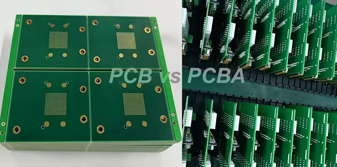
PCB vs PCBA

Selecting Copper Thickness for PCB Prototypes

  • By Frank guo
  • 2026年 9月 13日
  • PCB Assembly
  • No Comments
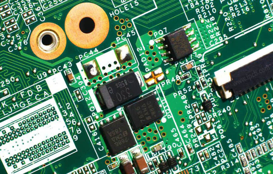
Selecting Copper Thickness for PCB Prototypes Copper thickness is specified in ounces, a unit inherited from the weight of foil used per square foot. One ounce copper is about thirty-five microns thick, and it is the default for most boards. Raising it changes what the board can carry, how it…

Continue Reading
Industrial IoT electronics

Why High Tg Material Matters in PCB Fabrication

  • By Frank guo
  • 2026年 9月 13日
  • PCB Assembly
  • No Comments
Why High Tg Material Matters in PCB Fabrication Every laminate has a temperature at which its mechanical behaviour changes. Below that point it is rigid and its dimensions are stable. Above it, the resin softens, expands faster and loses the stiffness that the rest of the process depends on. That…
Continue Reading
PCB Surface Treatment

Choosing Pad and Hole Sizes for PCB Prototypes

  • By Frank guo
  • 2026年 9月 13日
  • PCB Assembly
  • No Comments
Choosing Pad and Hole Sizes for PCB Prototypes Hole size looks like a trivial dimension. A lead of a known diameter goes into a hole of a slightly larger diameter, and the pad around it is drawn to suit. In practice the choice is constrained from both sides: the hole…
Continue Reading

PCB Panel Copper Distribution: Spreading It Evenly

  • By 杰夫
  • 2026年 9月 13日
  • PCB Assembly
  • No Comments
PCB Panel Copper Distribution: Spreading It Evenly Buyers and engineers often focus on the finished product and forget the production line behind it. In practice, most field failures can be traced back to process decisions made during assembly. Understanding PCB panel copper distribution gives you a practical advantage when you…
Continue Reading

PCB Copper Balancing Across Layers: Keeping the Panel Even

  • By 杰夫
  • 2026年 9月 13日
  • PCB Assembly
  • No Comments
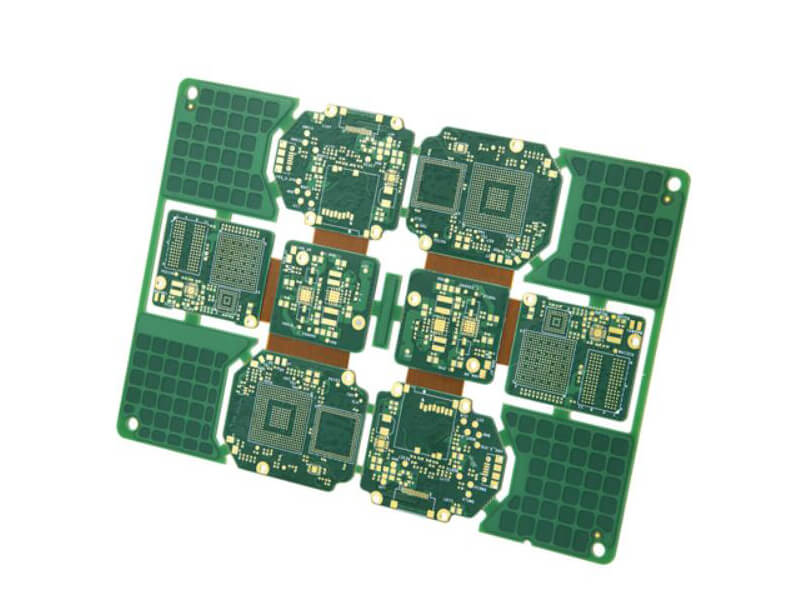
PCB Copper Balancing Across Layers: Keeping the Panel Even Modern electronics depend on boards that are assembled correctly the first time. Every product – a phone, a charger, a medical instrument or an industrial controller – relies on thousands of solder joints that must conduct current for years. This article…
Continue Reading

PCB Design Layers Explained: Signal, Plane, Mask, and Mechanical

  • By Frank guo
  • 2026年 9月 13日
  • PCB Assembly
  • No Comments
PCB Design Layers Explained: Signal, Plane, Mask, and Mechanical Modern layout software presents the design as a stack of named layers, and new engineers often find the number of them overwhelming. Each layer has a specific role, and each one produces a different output file or a different instruction to…
Continue Reading

PCB Production Process: Twelve Steps From Data to Final Test

  • By Frank guo
  • 2026年 9月 13日
  • PCB Assembly
  • No Comments
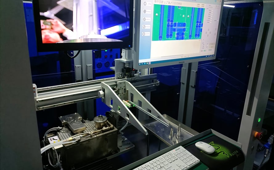
PCB Production Process: Twelve Steps From Data to Final Test A bare board is produced by a sequence of operations where each step depends on the accuracy of the one before it. The PCB production process begins with engineering data and ends with an electrical test, and the yield of…
Continue Reading
PCB Manufacturing

Metal Core PCB Design and DFM: Stackup, Vias and Grounding

  • By Frank guo
  • 2026年 9月 13日
  • PCB Assembly
  • No Comments
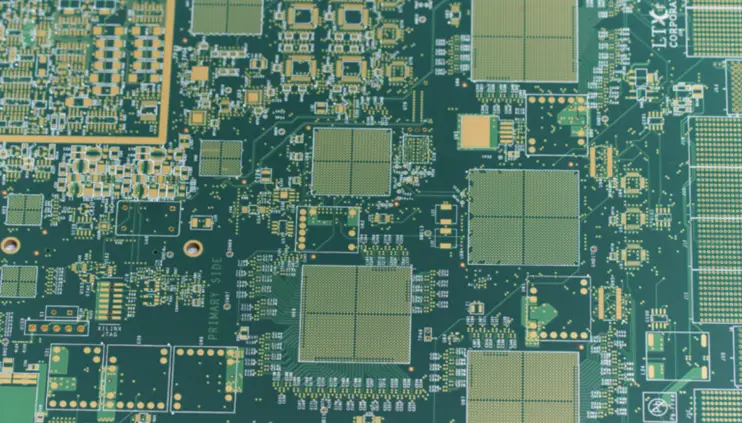
Metal Core PCB Design and DFM: Stackup, Vias and Grounding Metal core boards are rare in consumer products and everywhere in lighting, power conversion, industrial drives and aerospace equipment. The reason is simple: a high power stage produces heat that has to leave the package quickly, and a glass reinforced…
Continue Reading

PCB Etching Quality: Undercut, Etch Factor and Defects

  • By Frank guo
  • 2026年 9月 13日
  • PCB Assembly
  • No Comments
PCB Etching Quality: Undercut, Etch Factor and Defects PCB etching quality is decided long before the panel reaches the etcher, even though this is the step that finally reveals the circuit pattern. In a pattern plating process, a resist layer is plated onto the copper that must remain and the…
Continue Reading
project image

Solder Bead Defects in SMT Assembly: Causes and Fixes

  • By Frank guo
  • 2026年 9月 13日
  • PCB Assembly
  • No Comments
Solder Bead Defects in SMT Assembly: Causes and Fixes Solder beads are the small spheres of alloy that appear on an assembly surface after reflow, sitting beside a joint instead of being part of it. A single bead of 0.3 mm looks harmless on the bench, but once it breaks…
Continue Reading
1 … 1,066 1,067 1,068 … 1,626

Search Posts

Categories

  • Electronic Materials
  • Electronical Engineering
  • Industrial Control
  • PCB Assembly
  • PCB Design
  • PCB Manufacturing

Recent Posts

Cheap PCB Costs: PCB Design, PCB Manufacturing & SMT vs TH Guide

Cheap PCB Costs: PCB Design, PCB Manufacturing & SMT vs TH Guide

Jelly - 2026年 9月 30日
Cheap PCB Costs: PCB Design, PCB Manufacturing & SMT vs TH Guide

Cheap PCB Costs: PCB Design, PCB Manufacturing & SMT vs TH Guide

Jelly - 2026年 9月 30日
NPI Manufacturing Delays: PCB Design, PCB Manufacturing & EMS Guide

NPI Manufacturing Delays: PCB Design, PCB Manufacturing & EMS Guide

Jelly - 2026年 9月 30日

Tags

AOI inspection automotive electronics automotive PCBA quality automotive standards box build assembly component mounting component procurement component supplier conformal coating defect prevention DFM checks DFM review e-bom management electronic component shortage electronic manufacturing services electronic manufacturing standards Electronic Materials electronics design best practice electronics manufacturing capacity electronics sourcing high volume production industrial electronics insertion mount manufacturability review mass production quality mixed technology PCB PCBA inspection PCBA prototype PCBA turnkey PCBA volume pricing PCB Design PCB layout rules PCB Manufacturing PCB sourcing power electronics PCB printed circuit board prototype quick turn PCB reflow soldering SMT assembly quality SMT production solder paste inspection solder paste printing surface mount technology vehicle electronics wave soldering
GOPCBA-logo

As a professional China PCB assembly manufacturer, we provide a full range of electronic manufacturing services from PCB fabrication, PCBA to OEM/ODM, including PCB design, PCB layout, rapid PCBA prototyping, components procurement, SMT/ THT assembly, china pcb assembly, china pcb prototype, PCBA testing and box build assembly.

Linkedin Facebook-f X-twitter Youtube Instagram

PCB ASSEMBLY

  • Prototype PCB Assembly
  • Low Volume PCB Assembly
  • High Volume PCB Assembly
  • Turnkey PCB Assembly
  • SMT PCB Assembly
  • Through-Hole PCB Assembly
  • Mixed Technology PCB Assembly
  • Flex PCB Assembly

OUR SERVICES

  • PCB Design/Layout
  • PCB Manufacturing
  • Rapid PCBA Prototyping
  • Components Procurement
  • Conformal Coating
  • PCBA Testing
  • Box Build Assembly
  • Wire & Cable Harness Assembly

TECHNICAL SUPPORT

  • About Us
  • Quality Management
  • Artificial Intelligence PCBA
  • Industrial PCBA
  • IOT PCBA
  • Medical PCBA
  • Energy PCBA
  • Telecommunications PCBA

Copyright © 2026. Shenzhen Kingda Electronics Co., LTD  All rights reserved. 

  • Sitemap
  • Terms of Service
  • Privacy Policy
Zmdi Zmdi-email Phone-square Whatsapp Weixin
x

ABOUT US

Progressively maintain extensive infomediaries via extensible nich. Capitalize on low hanging fruit. a ballpark value added is activity to beta test. Override the digital divide with additional click throughs from fruit.

LOCATIONS

map

New York Office

+07 554 332 322
contact@example.com
office@example.com
37 San Fairport, NY 14450, New York City
All Locations

FOLLOW US