
Solder Bead Defects in SMT Assembly: Causes and Fixes
Solder beads are the small spheres of alloy that appear on an assembly surface after reflow, sitting beside a joint instead of being part of it. A single bead of 0.3 mm looks harmless on the bench, but once it breaks loose inside a powered product it can bridge two nets and take the unit down months after it shipped. Preventing solder bead defects is therefore a process control task rather than a cleaning task.
The beads come from three different mechanisms, and each needs a different fix. Paste that is printed in too large a volume squeezes out from under the component during reflow. Moisture trapped in the laminate or in a component body flashes to steam and throws molten alloy across the board. Mechanical splashing during hand soldering or rework scatters droplets that solidify where they land.
Why Solder Beads Matter
The risk is mechanical and hidden. A bead resting in the shadow of a component, under a shield can or inside a connector body will not appear in a normal top-down inspection, and it can migrate when the board is handled, vibrated or coated. Once it reaches a fine pitch pad row, it becomes a short that appears only at temperature or after a shock event, which is the worst class of field failure to diagnose.
Acceptance criteria treat loose solder balls above a defined diameter as a defect regardless of where they sit, and the threshold shrinks as pitch shrinks. A process that produces a few beads on a coarse board may be tolerable; the same process on a 0.4 mm pitch design is a yield and reliability problem.
Excess Solder Paste Volume
The most common cause of beading is simply too much paste on the pad. When the deposit is thicker than the gap between the pad and the component termination allows, the surplus is pushed sideways as the alloy melts and then balls up on the solder mask surface, where it cannot wet anything. Squeegee pressure, stencil wear, an unplanned aperture enlargement and paste that has thinned during a long print run all raise the deposited solder paste volume above the target.
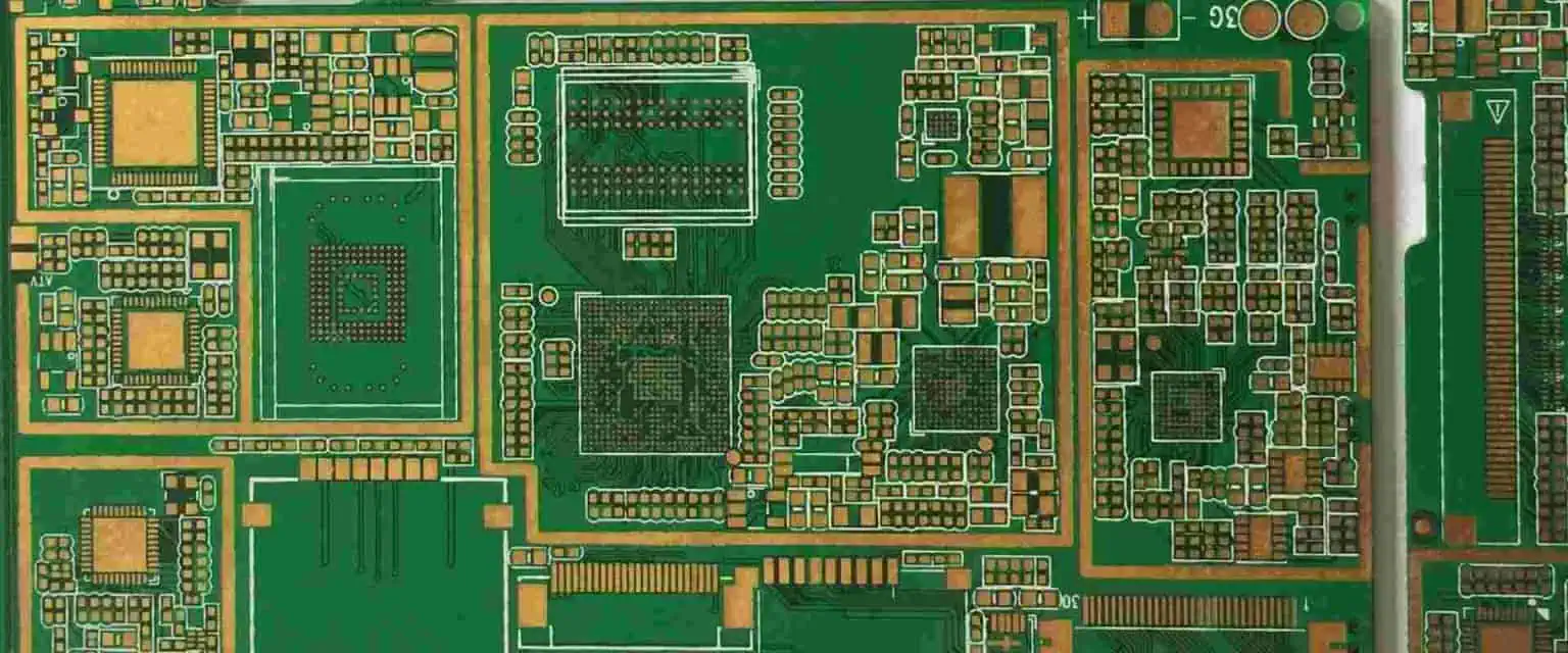
The stencil aperture is the first lever for correcting it. Openings larger than about 3 mm are normally split with a narrow bridge so that the printed area stays below the size at which the deposit slumps, and the area ratio of opening to wall controls how cleanly the paste transfers. Paste that sticks to the aperture wall and smears around the opening edge produces exactly the ragged deposit that generates beads later. The geometry rules are described in the notes on solder paste mask openings.
Moisture Absorption and Popcorning
Laminate and package bodies take up water from the air, and the amount depends on the material and on how it has been stored. When the assembly enters the reflow oven, that water turns to steam faster than it can escape. The pressure finds a path out through the molten joint and sprays alloy onto the surrounding surface. The same mechanism produces the delamination and internal cracks that give moisture absorption its reputation as a reliability issue rather than a cosmetic one.
Baking is the standard countermeasure. Boards and moisture sensitive components are dried before assembly, typically for two to eight hours at 120 to 125 degrees Celsius depending on thickness and on the moisture sensitivity level of the parts, and they are used within the floor life stated for that level. Boards that carry BGA, QFN or any package with a large body should be baked as routine, and partially used reels should be returned to dry storage rather than left on the line.
Reflow Splash from Flux Volatiles
Even a dry board can produce beads when the profile is wrong. A preheat that is too fast drives the solvent out of the paste before the flux has time to activate, and the escaping vapour carries paste particles away from the pad. That event is usually called reflow splash, and it leaves a ring of tiny spheres around the component footprint rather than a single large bead.
The cure is a slower ramp and a proper soak. Holding the assembly in the 150 to 180 degrees Celsius band long enough to activate the flux and evaporate the volatiles, then ramping to peak at a controlled rate, removes most of the driving force. Rework and second-side reflow cycles need their own profile rather than a repeat of the first pass, because the board enters the oven at a different temperature.
Hand Soldering and Rework
Manual work introduces a mechanical source that no paste control can fix. Flicking the iron to clear a tip, applying too much solder wire, or using a high-power iron on a small joint all throw droplets across the board. The droplets land on solder mask and stay there, and because hand soldering usually happens after the automated process, nothing downstream is looking for them.
Two controls make a measurable difference. Operators should wipe the tip on a brass cleaner instead of shaking it, and every board that has been touched by an iron should be inspected around the work area under magnification before it leaves the station. Post-solder visual checks documented in the assembly notes on design guidelines for manufacturability are a cheap way to formalise that step.
Squeegee Settings and Stencil Wear
Squeegee pressure and speed decide how much paste is pushed into the aperture and how much is smeared across the mask. Too little pressure leaves the opening partly filled, and the operator compensates by printing a thicker deposit; too much pressure wears the stencil and the squeegee edge, and the wear itself changes the release over the life of the tool. A worn squeegee with a rounded edge is a frequent cause of a beading problem that appears gradually across a production week.
Stencil condition deserves the same attention. Nano-coated foils release paste more cleanly than untreated ones and hold the benefit longer, while a foil that has been cleaned aggressively with a metal scraper loses its taper. Recording the number of print cycles on each stencil and inspecting the fine pitch apertures at a fixed interval turns a slow drift into a scheduled maintenance item.
Removal and Cleaning
Beads that are already present have to be removed rather than redistributed. Dry brushing and compressed air move them into places where they are harder to see. A soft brush with a solvent matched to the flux chemistry lifts them off the mask, and the board is then cleaned in the normal wash if the process includes one. Any bead found under a component body should be treated as a failure of the process rather than a housekeeping problem, because it cannot be verified as removed.
Process Controls That Prevent Beads
Prevention is built from a small set of measurements. Solder paste inspection gives the deposit volume on every pad, so an upward trend is visible before defects appear. The stencil should be wiped on a defined cycle, and the aperture condition checked when the wipe frequency has to be increased. Paste should be used within its working life, stirred to specification and never topped up with fresh material in the same container.
The last consideration is the coating step. A bead trapped beneath a layer of conformal coating for board protection is fixed in place and hidden permanently, which is why inspection has to happen before coating and not after.
Inspection
Automated optical inspection detects beads reliably on visible surfaces but not in shadowed areas, so the inspection programme should include a magnified manual check of connector bodies, shield frames and component sides. X-ray adds little for beading because the beads are not inside a joint, so the effort is better spent on the paste volume data and on the profile records.
FAQ
Can solder beads be prevented by cleaning after reflow? Cleaning removes beads that are already on the surface. Prevention comes from controlling paste volume, moisture and the reflow profile.
Why do beads appear only on some boards in a lot? Usually because the paste deposit drifts during the print run or because part of the lot absorbed moisture. Comparing paste volume data with the bake records identifies which one applies.
Are small beads between fine pitch pads acceptable? No. At fine pitch a bead is large enough to bridge two pads, so any loose alloy in that region is treated as a defect.