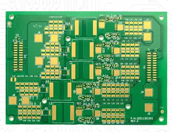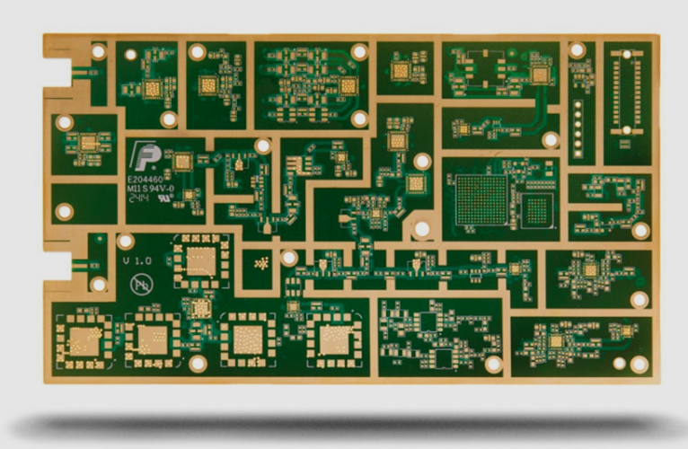
POFV Process in PCB Fabrication: Plated Over Filled Via Fine-pitch ball grid array packages and stacked microvia structures have made one question unavoidable in HDI fabrication: what happens to the via after it is filled? If the via is left open, the pad above it is not flat and the…

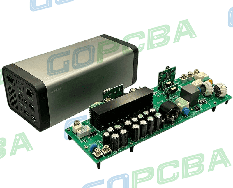
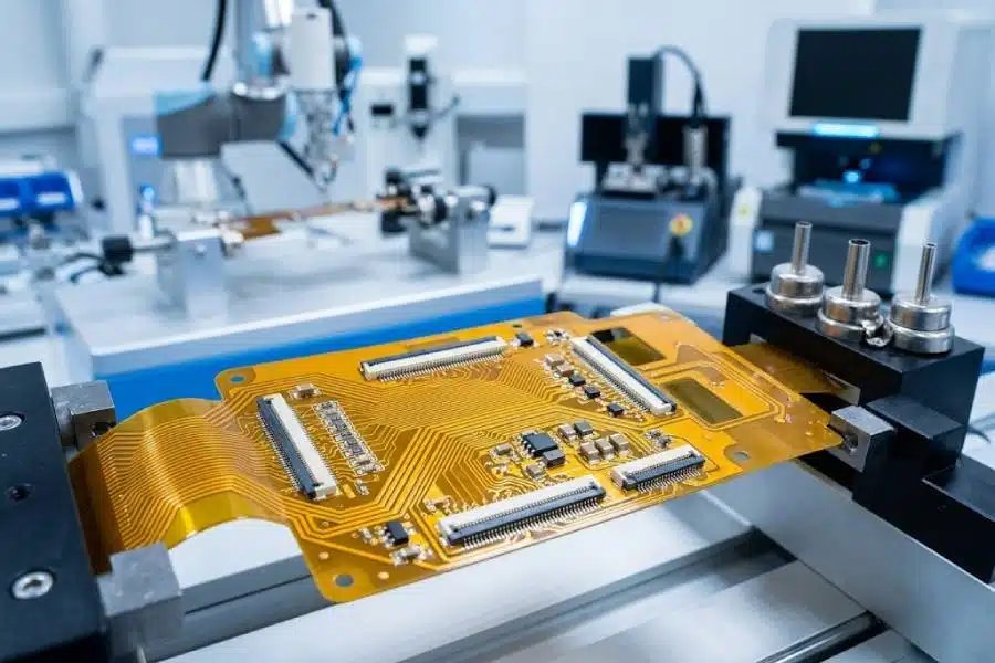
PCBA Assembly Methods for Single-Sided and Double-Sided Boards The assembly route for a board is decided long before the first unit is built, and it is usually fixed by the mix of components the design contains. A board with only surface-mount parts follows one path, a board with a handful…
PCB Microsection Preparation: Grinding to the Truth Electronics manufacturing has become a discipline of small details. Solder paste volumes, placement accuracy, temperature profiles and inspection limits all add up to the final result. This guide looks at PCB microsection preparation from the perspective of a PCBA factory floor, covering cutting…
PCB Surface Insulation Resistance Testing: Watching the Leakage Electronics manufacturing has become a discipline of small details. Solder paste volumes, placement accuracy, temperature profiles and inspection limits all add up to the final result. This guide looks at PCB surface insulation resistance testing from the perspective of a PCBA factory…
Parallel Bus and Serial Bus Routing Rules for PCB Layout Almost every high-speed interface on a modern board is either a parallel bus or a serial bus, and the two families fail for different reasons. A parallel bus fails when one lane arrives at the wrong time; a serial bus…
PCB Spark Gap Design for On-Board ESD Protection Static discharge remains one of the few failure mechanisms that can destroy a board before it is ever powered. The conventional answer is a protection component placed between the connector and the circuit, but a component adds cost, consumes board area and…
Building a BOM for SMT Prototype Assembly On an SMT prototype build, the BOM is not a purchasing document that sits beside the design. It is the data set the placement machine is programmed from, the list incoming inspection checks against, and the file that decides whether the build can…
PCB Ionic Contamination Testing: What the Rinse Left Behind Buyers and engineers often focus on the finished product and forget the production line behind it. In practice, most field failures can be traced back to process decisions made during assembly. Understanding PCB ionic contamination testing gives you a practical advantage…
PCB Routing Strategy: Corners, Differential Pairs and Serpentines Routing is where the theory of high-speed design either survives or dies. A stackup can be textbook-clean and the schematic can be perfect, but if the traces are laid down carelessly the board will still miss its timing window or fail EMC.…
Via Plugging Process Control for PCB Assembly A via is drilled and plated to connect layers, but on a finished board it is also a hole in the surface that solder, flux and cleaning chemistry can enter. The via plugging process exists to close that hole in a controlled way,…