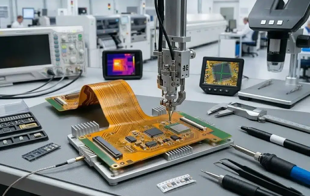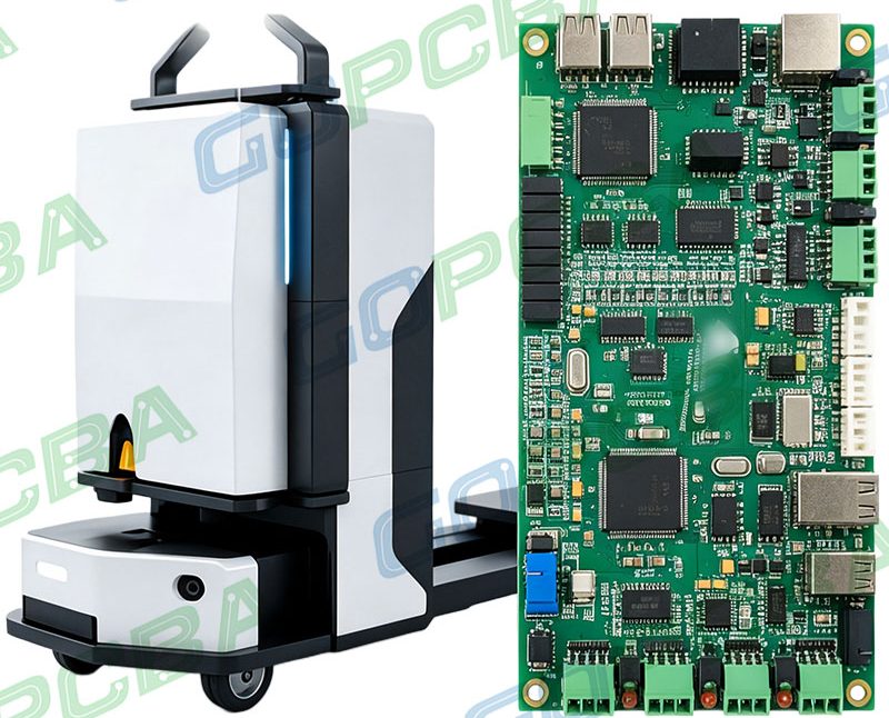
PCB Manufacturing Automation and Process Optimization Circuit board production has become a data-driven process. Design files are converted into tooling automatically, panels are imaged with laser direct imaging instead of film, and every board carries a traceable history of the process parameters that produced it. The shift matters commercially because…
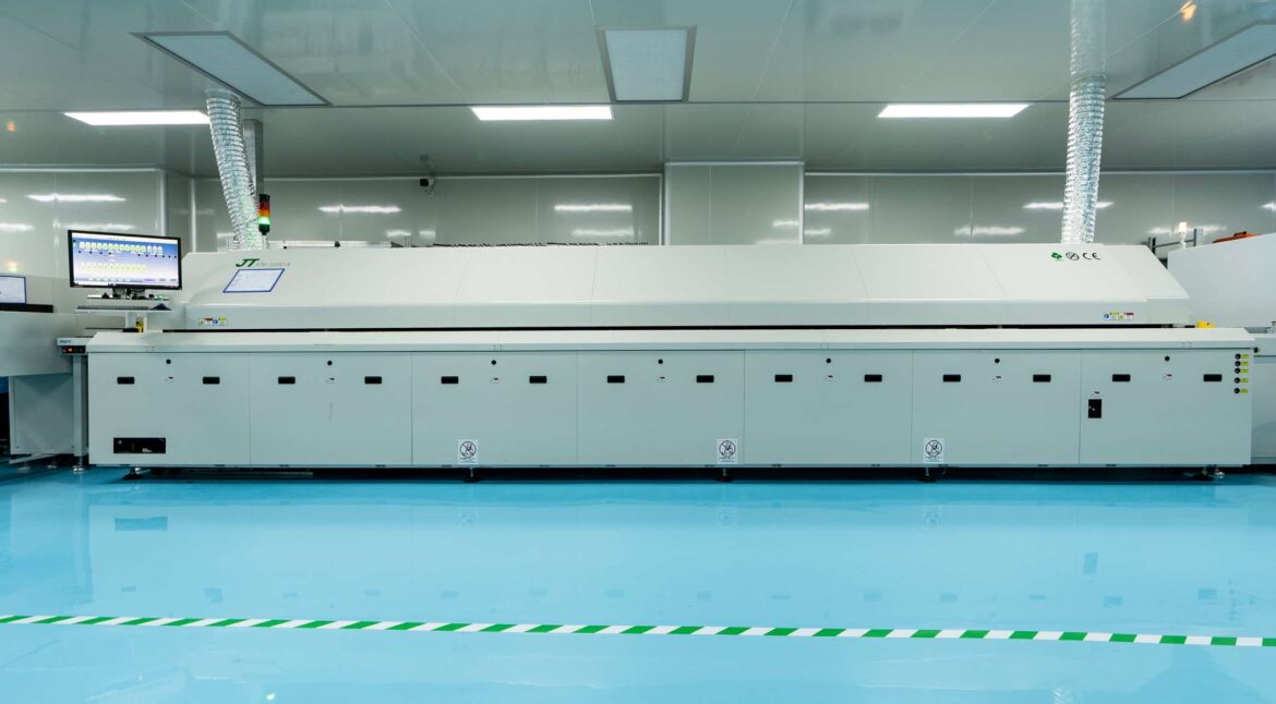
PCB Layout Design Rules for Manufacturable Boards Most layout rework is not a routing problem. It is a rule problem: a pad whose annular ring is too thin, a trace that runs too close to the routed profile, or a solder mask dam that disappears after etch compensation. Fabricators work…
Automotive PCBA Design: Assembly Spacing, Reflow, and Test Rules Automotive assemblies are built to a stricter floor than consumer products, and most of that strictness lands on details that are decided during layout rather than during electrical design. Component spacing, reflow exposure, test access, and copper thickness all have to…
HDI Board Versus Standard PCB: Microvia, Laser Drilling, and Cost Two boards can have the same layer count and the same outline and still be completely different products. The difference is whether the interconnections between layers are made with through holes only, or with a build-up structure that uses blind…
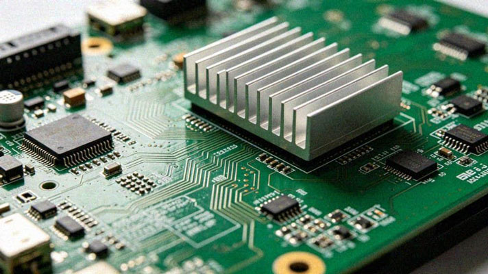
AI Mainboard PCB Design and Fabrication: Materials, Process and Test Accelerator cards, edge inference appliances and AI servers all share the same physical problem: a very large processor package that has to be fed with clean power, kept cool and connected to memory and peripherals at rates that leave almost…
AI Smartphone PCB Design: Compute Density, Signals and Heat Smartphones stopped being simply “smart” once they began running inference locally. Adding a neural processing unit to an application processor changes far more than the bill of materials: it turns the main board into a compute platform where every square millimetre…
MCU Control Board Layout: Decoupling and Grounding Rules A microcontroller control board for a small appliance looks simple: an MCU, a few driver stages, a display, some buttons and a power supply. In practice it is one of the harder boards to get right, because the same board carries switching…
PCB Layout Design: A Practical Workflow from Schematic to Gerber PCB layout design is often described as drawing connections between components, but the drawing is the last part of the job. By the time a designer starts routing, the electrical behaviour of the board has already been shaped by the…
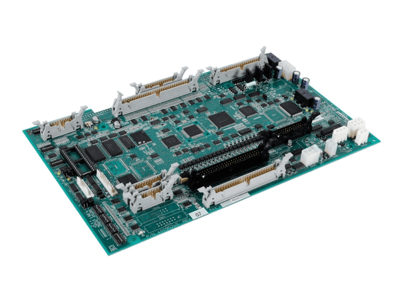
PCB Design vs PCBA: What the Difference Means for a Build Ask two engineers what the difference is between PCB design and PCBA and the answers will often describe the same object from different ends of the process. One is a bare board with copper, mask and silkscreen. The other…
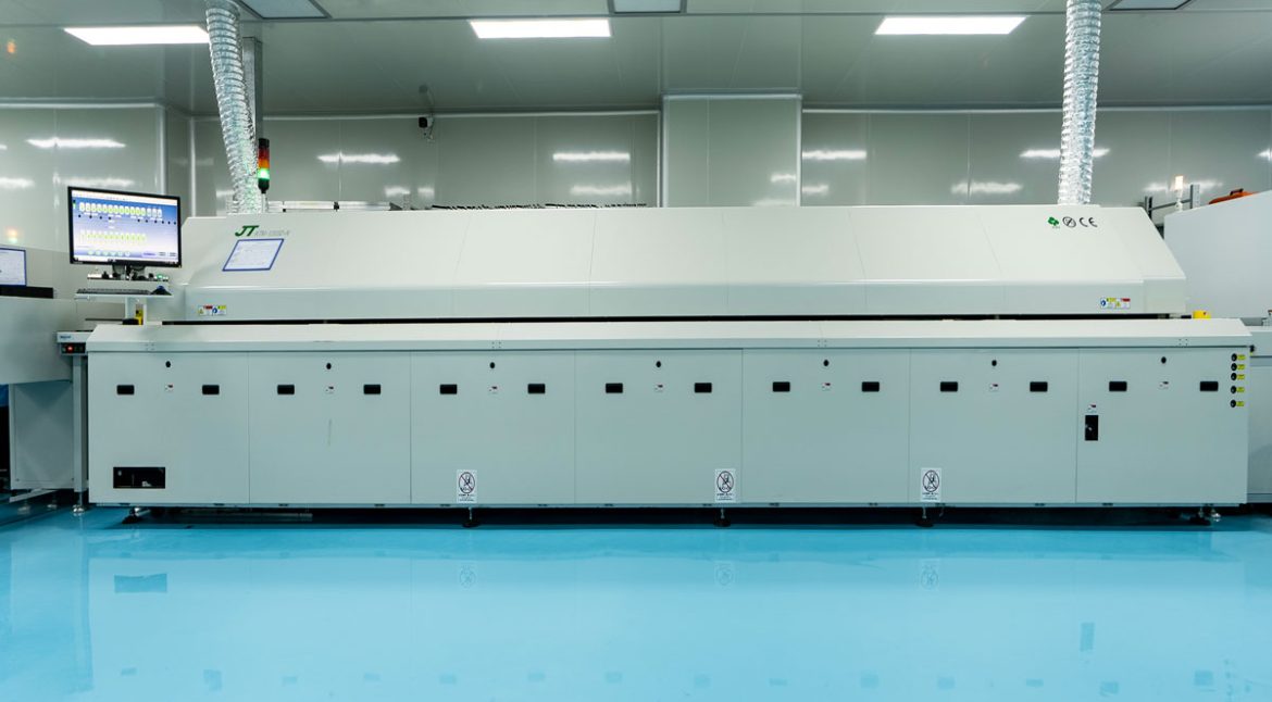
PCB Process Validation for A New Line: Before the Line Is Released Buyers and engineers often focus on the finished product and forget the production line behind it. In practice, most field failures can be traced back to process decisions made during assembly. Understanding PCB process validation for a new…