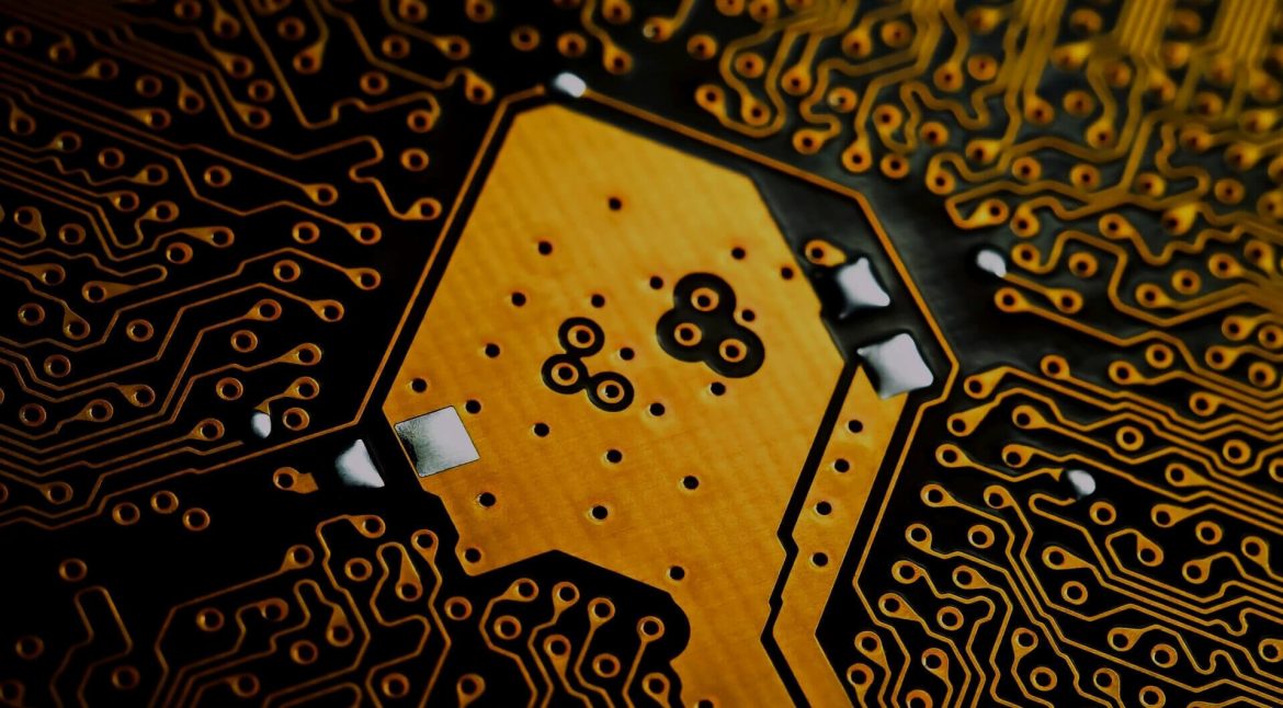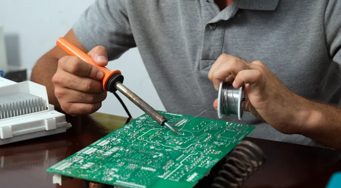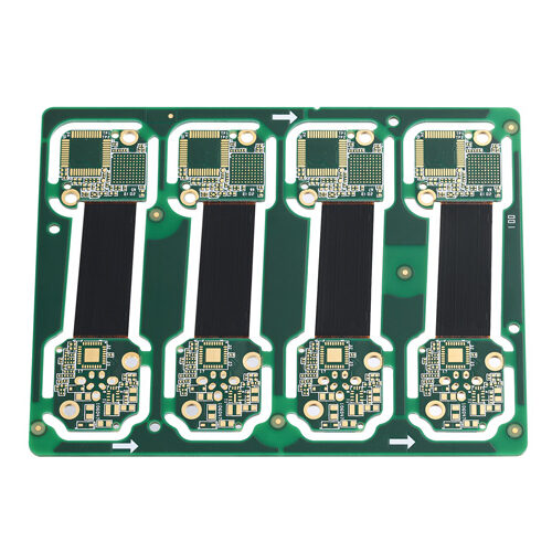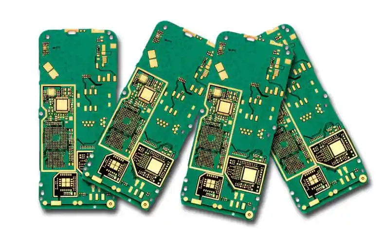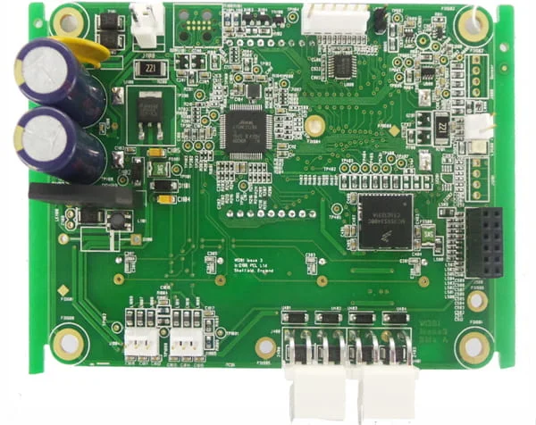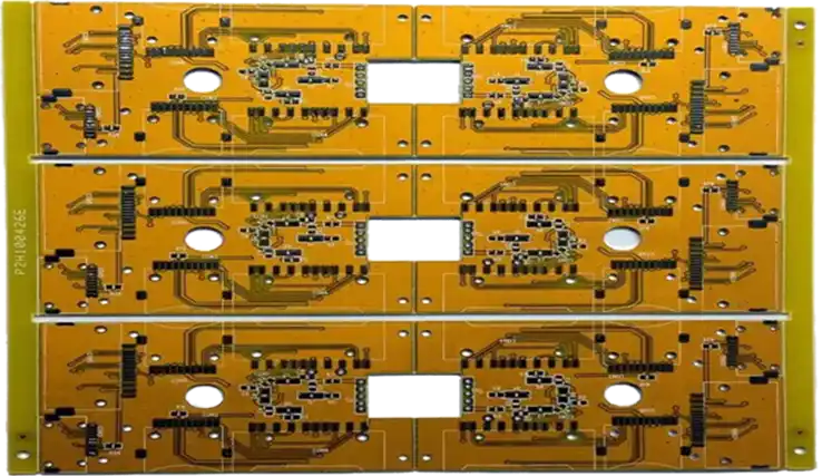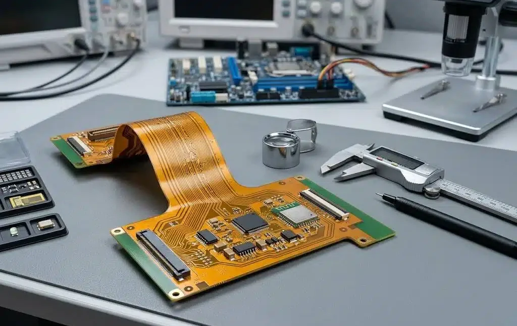
Multilayer PCB Advantages in High Speed Design Once a design contains signals whose edges are fast relative to the length of the traces they travel along, the board stops being a container for wires and becomes part of the circuit. At that point the number of layers stops being a…
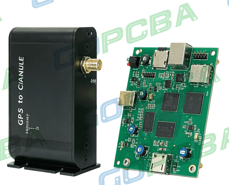
PCB Edge Plating for Shielding: Copper Around the Rim Buyers and engineers often focus on the finished product and forget the production line behind it. In practice, most field failures can be traced back to process decisions made during assembly. Understanding PCB edge plating for shielding gives you a practical…
PCB Gold Finger Bevel and Chamfer: Getting the Edge In Electronics manufacturing has become a discipline of small details. Solder paste volumes, placement accuracy, temperature profiles and inspection limits all add up to the final result. This guide looks at PCB gold finger bevel and chamfer from the perspective of…
PCB Hard Gold Versus ENIG for Connectors: Gold for the Edge Electronics manufacturing has become a discipline of small details. Solder paste volumes, placement accuracy, temperature profiles and inspection limits all add up to the final result. This guide looks at PCB hard gold versus ENIG for connectors from the…
PCB OSP Storage Conditions: A Film That Ages Modern electronics depend on boards that are assembled correctly the first time. Every product – a phone, a charger, a medical instrument or an industrial controller – relies on thousands of solder joints that must conduct current for years. This article explains…
PCB Immersion Silver Tarnish Control: Keeping It Bright Buyers and engineers often focus on the finished product and forget the production line behind it. In practice, most field failures can be traced back to process decisions made during assembly. Understanding PCB immersion silver tarnish control gives you a practical advantage…
PCB Design Quality: The Characteristics That Matter Two boards can satisfy the same schematic and behave completely differently in the field. The difference is design quality, and it is not a single property but a set of them, each of which can be assessed before the board is built. The…
PCB ENIG Black Pad Diagnosis: When the Gold Goes Wrong Electronics manufacturing has become a discipline of small details. Solder paste volumes, placement accuracy, temperature profiles and inspection limits all add up to the final result. This guide looks at PCB ENIG black pad diagnosis from the perspective of a…
PCB Design and PCB Fabrication Working Together Design and fabrication are usually described as consecutive steps, as though the designer finishes and the fabricator begins. In practice they are a loop. The design determines what the fabricator has to achieve, and the fabricator”s capability determines what the design can ask…
PCB Surface Finish Shelf Life Comparison: How Long It Lasts Electronics manufacturing has become a discipline of small details. Solder paste volumes, placement accuracy, temperature profiles and inspection limits all add up to the final result. This guide looks at PCB surface finish shelf life comparison from the perspective of…