Shielding Methods for High-Speed PCB Design As data rates rise, the signals that carry the data become more sensitive and their energy becomes smaller at the same time. A fast edge spends a very short time at each level, and the receiver has to decide what it saw from a…
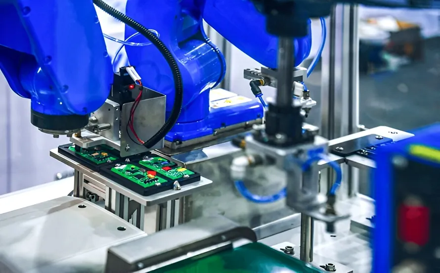
PCB Aging Test for Power Boards: Proving the Supply Lasts Electronics manufacturing has become a discipline of small details. Solder paste volumes, placement accuracy, temperature profiles and inspection limits all add up to the final result. This guide looks at PCB aging test for power boards from the perspective of…
How to Tell a High-Speed Signal from a Low-Speed One in PCB Design The question of which signals on a board are high speed and which are not comes up in every layout review, and it is usually answered with the clock frequency. That answer is wrong often enough to…
PCB Burn in Test Procedure: Running the Board Hot Modern electronics depend on boards that are assembled correctly the first time. Every product – a phone, a charger, a medical instrument or an industrial controller – relies on thousands of solder joints that must conduct current for years. This article…
Importing and Updating a Netlist in PCB Layout The transfer from a schematic to a layout is where a design stops being a drawing and starts being a physical object, and the netlist is the document that carries the intent across. Every change after that transfer travels the same route,…
PCB Test Socket Selection: Choosing the Socket for the Part Electronics manufacturing has become a discipline of small details. Solder paste volumes, placement accuracy, temperature profiles and inspection limits all add up to the final result. This guide looks at PCB test socket selection from the perspective of a PCBA…
Adding a Logo on a PCB: Silkscreen Versus Copper Artwork A logo or a marking on a board is a small feature with a surprising number of ways to go wrong. It shares space with pads and vias, it has to survive the assembly process, and it has to be…
PCB Test Probe Maintenance: Keeping the Contact Clean Electronics manufacturing has become a discipline of small details. Solder paste volumes, placement accuracy, temperature profiles and inspection limits all add up to the final result. This guide looks at PCB test probe maintenance from the perspective of a PCBA factory floor,…
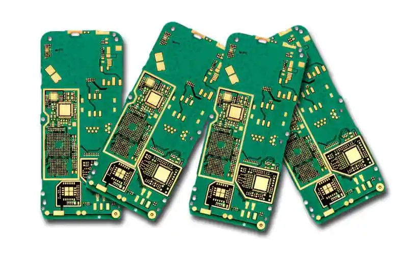
Anatomy of a Printed Circuit Board: Pads, Vias and Layer Types A printed circuit board looks like a single object, but it is a stack of different materials and a set of features that each do one job. Knowing what those features are called and what they are for makes…
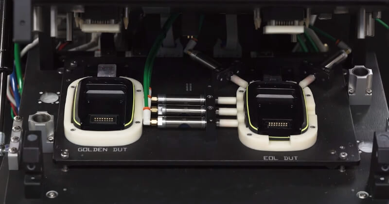
PCB Fixture Pin Wear: When the Probes Get Tired Buyers and engineers often focus on the finished product and forget the production line behind it. In practice, most field failures can be traced back to process decisions made during assembly. Understanding PCB fixture pin wear gives you a practical advantage…