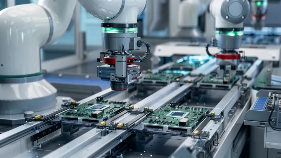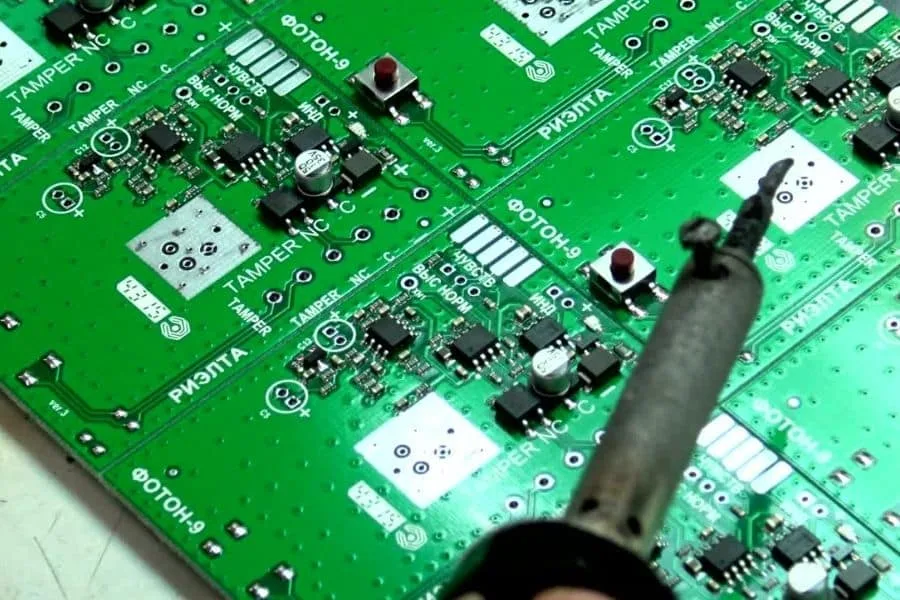
PCB Potting Void Control: Keeping Air Out of the Potting Buyers and engineers often focus on the finished product and forget the production line behind it. In practice, most field failures can be traced back to process decisions made during assembly. Understanding PCB potting void control gives you a practical…
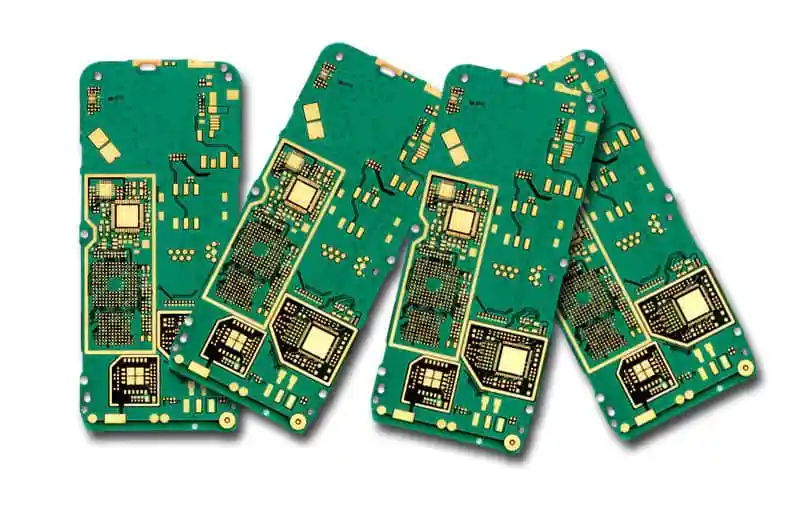
PCB Design Mistakes: The Errors That Reach Production Most of the errors that stop a board from being built are not electrical. They are documentation and geometry mistakes that pass a design rule check because no rule covers them, and they surface when the fabrication data is processed or when…
PCB Coating Rework and Touch Up: Repairing a Damaged Coat Buyers and engineers often focus on the finished product and forget the production line behind it. In practice, most field failures can be traced back to process decisions made during assembly. Understanding PCB coating rework and touch up gives you…
PCB Quality Inspection: What You Can Judge Without a Microscope Not every quality question requires a laboratory. When a batch of bare boards arrives, several of the characteristics that separate a controlled process from an approximate one are visible to the naked eye, or with modest magnification. None of them…
PCB Coating Cure Profile: Setting the Heat for the Film Modern electronics depend on boards that are assembled correctly the first time. Every product – a phone, a charger, a medical instrument or an industrial controller – relies on thousands of solder joints that must conduct current for years. This…
PCB Drilling Defects: Hole Wall Debris and Oversized Holes Two of the most common drilling defects in PCB fabrication look unrelated but come from the same family of causes. One is debris left on the wall of the hole, which interferes with plating and produces a connection that is weak…
PCB Coating Adhesion Test: Checking the Film Sticks Buyers and engineers often focus on the finished product and forget the production line behind it. In practice, most field failures can be traced back to process decisions made during assembly. Understanding PCB coating adhesion test gives you a practical advantage when…
Parasitic Elements in PCB Design: Stray Capacitance and Inductance Every trace on a board is a component. It has resistance, it has capacitance to whatever is next to it or beneath it, and it has inductance along its length. The designer did not place these elements, which is exactly why…
Backplane Design: Thick Boards, Press-Fit Connectors and Stubs A backplane is the board that connects everything else. It carries little or no active circuitry, it is often the thickest board in the system, and it is expected to survive being assembled once and then working for a decade. Designing one…
Ground Plane Splitting: When It Helps and When It Hurts Separating the analogue ground from the digital ground is one of the most widely repeated pieces of advice in hardware design, and it is also one of the most widely misapplied. The reasoning behind it is sound: digital circuits switch…