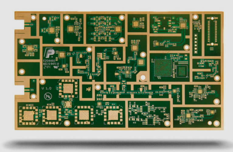
PCB Silkscreen Data: What the Numbers Say Buyers and engineers often focus on the finished product and forget the production line behind it. In practice, most field failures can be traced back to process decisions made during assembly. Understanding PCB silkscreen data gives you a practical advantage when you choose…
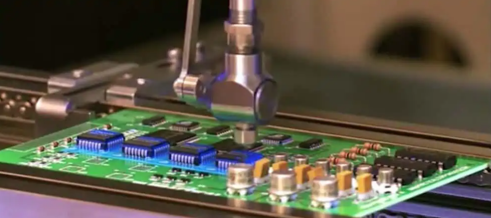
Panel Fiducial and Tooling Strategy for PCB Assembly A placement machine finds the board by looking for marks printed on it. Those marks are fiducials, and the holes that locate the panel in the machine are tooling holes. Both belong to the design, and a board with poorly specified references…
Metal Core PCB Thermal Design A metal core board replaces the usual glass reinforced laminate with a metal base, normally aluminium, covered by a thin dielectric layer and the copper circuit. The construction takes the heat that a component generates and spreads it across the whole board area, which lowers…
Board Support and Backing Systems for Reliable SMT Assembly A printed circuit board is flat when it is manufactured and flexible when it is being processed. In a printer, a placement machine or a reflow oven the board is pushed, pressed and heated, and it will bend unless something holds…
PCB Silkscreen Limits: Where the Edges Are Electronics manufacturing has become a discipline of small details. Solder paste volumes, placement accuracy, temperature profiles and inspection limits all add up to the final result. This guide looks at PCB silkscreen limits from the perspective of a PCBA factory floor, covering understanding…
PCB Silkscreen Setup: Getting Ready Modern electronics depend on boards that are assembled correctly the first time. Every product – a phone, a charger, a medical instrument or an industrial controller – relies on thousands of solder joints that must conduct current for years. This article explains PCB silkscreen setup…
PCB Silkscreen Maintenance: Keeping It Working Electronics manufacturing has become a discipline of small details. Solder paste volumes, placement accuracy, temperature profiles and inspection limits all add up to the final result. This guide looks at PCB silkscreen maintenance from the perspective of a PCBA factory floor, covering maintaining silkscreen…
Backdrilling: Preparation, Placement and Process Control Backdrilling is the controlled removal of the unused portion of a plated through hole. A via that runs the full thickness of a thick board leaves a stub below the layer where the signal joins, and at high frequency that stub behaves as a…
Cavity Board Design Guide A cavity board carries a recess in the laminate so that a component can sit below the surface, either to keep the overall height within a limit or to bring a sensor or an optical part closer to the outside face. The cavity is produced by…
Blind Via Filling Guide A blind via connects an outer layer to an inner layer and stops without passing through the board. When another via has to be placed directly above it, or when the via lies in a pad that must be printed flat, the hole has to be…