Decoupling Capacitor Placement in HDI Boards with BGA Packages Decoupling capacitor placement used to be a routine task. The designer put a small capacitor next to every power pin, tied it to the ground plane with a short via, and moved on. In a modern high density interconnect board carrying…
Flexible Circuit Materials And Construction A flexible circuit is not a thin rigid board. It is a different construction with different materials, and the rules that govern it are written by mechanics rather than by impedance. Understanding the stackup is the first step towards designing one that survives being bent.…
PCB Copper Bar for High Current: Metal Bolted to the Board Buyers and engineers often focus on the finished product and forget the production line behind it. In practice, most field failures can be traced back to process decisions made during assembly. Understanding PCB copper bar for high current gives…
Snubber Circuits and Their PCB Layout Every switching circuit contains inductance that the designer did not intend. The loop formed by the transistor, the diode, and the capacitor has a parasitic inductance measured in nanohenries, and when the current is interrupted the energy stored in that inductance has to go…
Inrush Current Limiting on Power Supply Boards Switch on a power supply and the input capacitor is empty. For a few milliseconds it looks like a short circuit, and the current that flows is limited only by the source impedance and the resistance of the wiring. The surge can be…
Aluminium Nitride: Design Rules and Process Limits Alumina has been the default ceramic substrate for decades because it is inexpensive, well understood and adequate for most applications. Aluminium nitride exists because alumina’s thermal conductivity is modest, and a substrate that insulates electrically while conducting heat is exactly what a power…
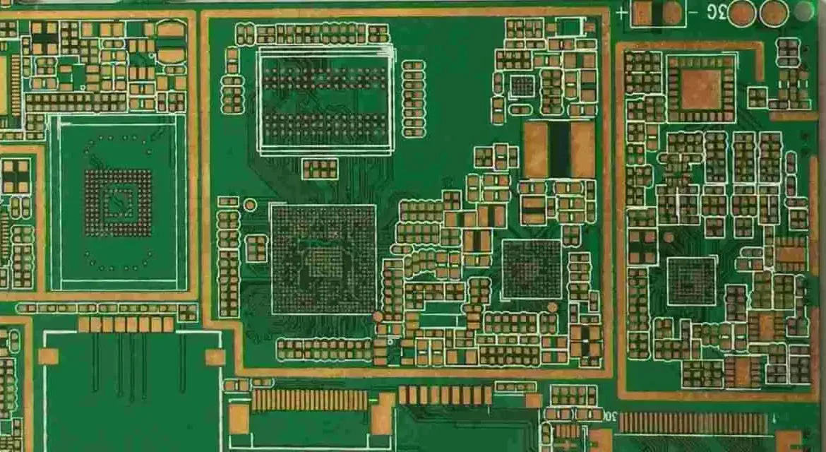
Five-Order Blind Via HDI Boards: Process Flow and Control A five-order blind via board is the point at which high density interconnect stops being a variation on conventional multilayer fabrication and becomes a separate discipline. Each order of blind via adds one more sequential lamination cycle, one more laser drilling…
Multilayer PCB Design: Rules That Hold Up in Production A multilayer PCB is not simply a double-sided board with extra layers. The added layers are a resource that has to be allocated deliberately, and the decisions made in the first hour of layout, about size, layer count and placement, are…
Thermal Via Design and Copper Spreading Under Power Devices A power device converts a fraction of its current into heat, and that heat has to leave the package through the board or through a heat sink. Where the primary path is the board, the design of the copper beneath the…
Copper Thickening In DPC Ceramic Substrates Direct plated copper substrates begin as a thin sputtered seed layer on a ceramic surface, which is enough to carry a circuit but not enough to carry tens of amperes. Thickening that layer by electroplating is what turns the process into one suitable for…