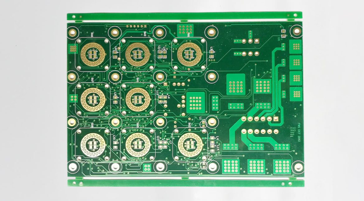
PCB Surface Finish Selection: Four Requirements Selecting a surface finish is a decision that is made once and affects the board for its whole life, because the finish determines how the board stores, how it solders and how its joints behave in service. The options are well characterised, and the…
Via Tenting Versus Via Exposure on a PCB The vias on a finished board are either covered by the solder mask or left open, and the choice is rarely made deliberately. It is inherited from a template, or copied from the previous product, or decided by whoever generated the fabrication…
Balanced Copper in PCB Design A finished panel that is not flat is difficult to assemble and impossible to solder reliably. The board may bow along one axis, twist about a diagonal, or simply refuse to sit flat in a fixture, and the cause is usually the way copper was…
IBIS Model Corner Parameters and How to Use Them An IBIS model describes the electrical behaviour of an input or output buffer without revealing the transistor level design, and it is the standard way a device vendor supplies information for signal integrity analysis. Reading the model correctly means understanding that…
Signal and Power Integrity Analysis for 3D IC Packages For most of the history of integrated circuit design, a system was built from a monolithic device mounted on a package and soldered to a board, and the signal and power integrity work divided neatly along those boundaries. The chip, the…
BGA Solder Void Causes and Acceptance Criteria Guide Solder voids appear in almost every X-ray image of a ball grid array, and almost every discussion about them ends in an argument about limits. The useful question is not whether voids exist but where they sit, how they formed, and whether…
PCB Coupon Location on A Panel: Where the Sample Sits Electronics manufacturing has become a discipline of small details. Solder paste volumes, placement accuracy, temperature profiles and inspection limits all add up to the final result. This guide looks at PCB coupon location on a panel from the perspective of…
Controlled Impedance: RF PCB Layout: Impedance, Grounding and Antenna Interfaces Radio frequency design on a printed circuit board is governed by a small number of rules that are easy to state and difficult to satisfy, because the layout must control an impedance, contain a field and reject a coupling, all…
Electroless Nickel Thickness Control and Black Pad Risk Electroless nickel immersion gold is the most widely used finish on fine pitch boards, and it is also the finish with the most misunderstood failure mode. The gold layer gets the attention, but the electroless nickel beneath it carries the load, defines…
Bare Board Shelf Life and Storage Conditions A printed circuit board is not an inert object. The laminate absorbs moisture, the finish oxidises, and the solder mask continues to cure. A board that has been stored badly for six months can be harder to assemble than a fresh one, and…