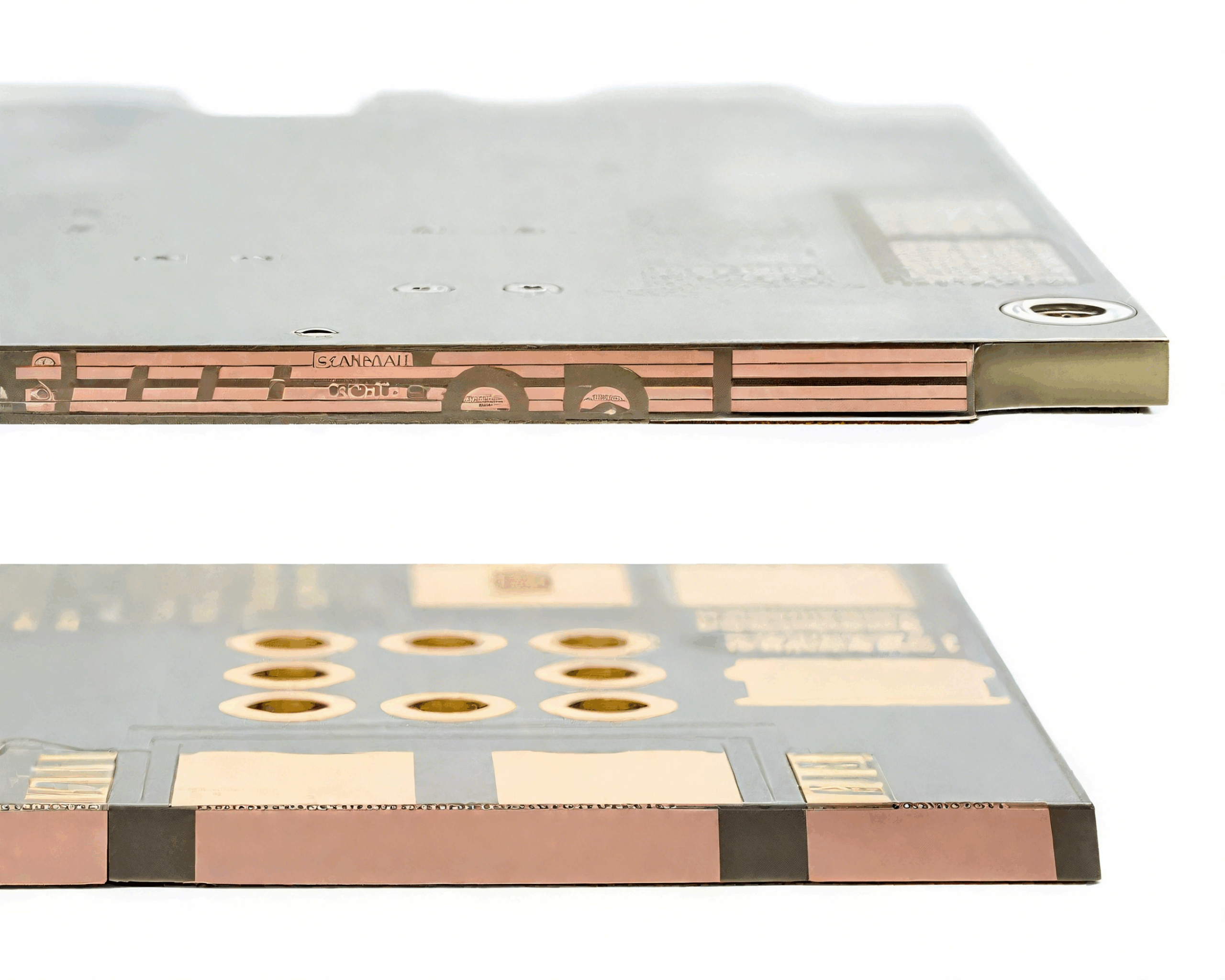
Solder Mask Process and PCB Reliability Solder mask is the least analysed layer on a printed circuit board and the one most often blamed for failures that appear months after delivery. It is applied after the copper is finished, it is cured at high temperature, and it has to survive…
Bill of Materials Control for PCB Assembly A bill of materials is a controlled document, and the discipline that keeps it correct is the same discipline that keeps the fabrication data correct. Where it is weak, the assembly line builds whatever the machine finds on the feeder, and the difference…
PTFE PCB: Low-Loss Laminate for High Frequency RF Boards A PTFE PCB is built on a polytetrafluoroethylene laminate rather than the usual woven-glass epoxy, and it exists because ordinary FR-4 runs out of performance somewhere above a few gigahertz. The material behaves differently at every stage: how it is drilled,…
Layer Count: What Drives PCB Cost: The Levers That Matter The cost of a printed circuit board is built up from a small number of cost drivers, and almost all of them are decided by the design rather than by the purchasing discussion. Knowing which lever moves which part of…
How Much Test Coverage Do You Actually Have? Test coverage is easy to assume and hard to prove, and the gap between the two is where escaped defects live. Building a defensible coverage argument requires understanding what each test can and cannot see, and where the boundaries between them fall.…
Hatched or Solid Copper Pour on a PCB Copper pour is the most common feature on a printed circuit board and one of the least examined. Designers pour copper because it is expected, choose between a grid and a solid fill from habit, and rarely ask what the fill is…
ICT And Functional Test For Assembled Boards Testing an assembled board is a question of what can be verified, at what cost, and at which point in the process. In circuit test checks the electrical continuity and isolation of the connections a board is supposed to have, and functional test…
Test Point: Bring-Up Provisions That Belong in the PCB Layout Every board has nodes that are difficult to reach and features that are easy to get wrong, and the cost of the difficulty is paid at first article, when the schedule is tightest. A design review that anticipates those nodes…
ESD Control in PCB Assembly Lines and Handling Areas A technician crosses a carpeted floor, touches a board, and a device inside it is quietly weakened. Nothing looks wrong, the assembly passes test, and the failure appears weeks later at a customer site. That is the nature of electrostatic discharge…
Connector Bandwidth: Where The Channel Really Ends A channel is usually analysed as a trace with a driver at one end and a receiver at the other, and the connector is treated as a detail. At high data rates that treatment is wrong. The connector often contributes more loss and…