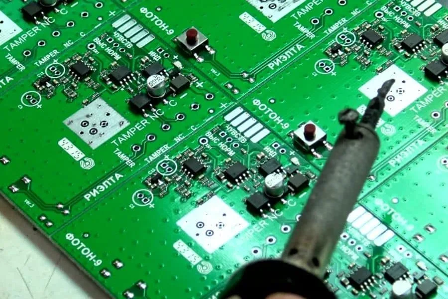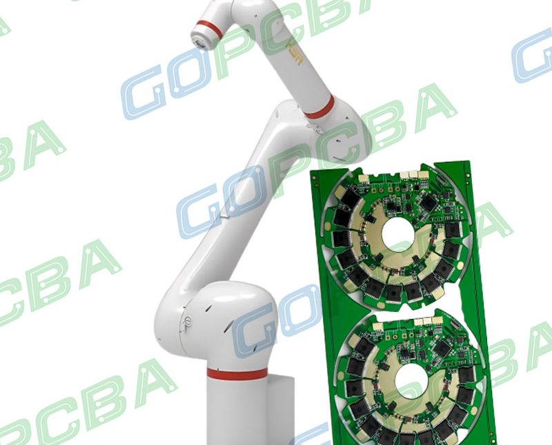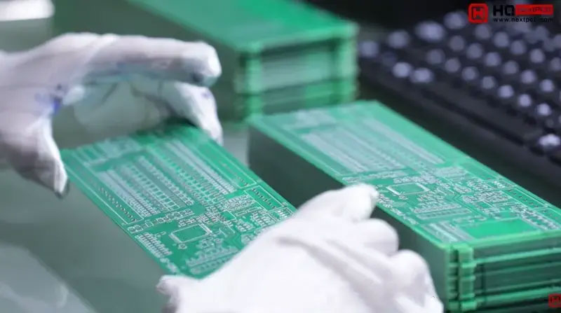
PCB Depanelling Methods: Separating Boards Safely Buyers and engineers often focus on the finished product and forget the production line behind it. In practice, most field failures can be traced back to process decisions made during assembly. Understanding PCB depanelling methods gives you a practical advantage when you choose a…

Flexible PCB Thickness: Choosing Between 0.05 mm and 0.5 mm Thickness is the first number anyone asks about a flexible circuit and the last one that gets designed properly. It decides how tightly the board can bend, whether it can survive being bent repeatedly, whether it will feed through an…
EMC and EMI Control in PCB Design: Practical Rules Electromagnetic compatibility is rarely decided by a single component. It is decided by the shape of the current paths on the board, and those paths are laid out long before anyone runs a compliance test. Every signal that leaves a driver…
Pad Design Criteria for Reliable Solder Joints A pad is the only place where the board and the component are physically joined, and it is sized and shaped by a set of rules that are less about the electrical design than about the soldering process. A pad that is too…
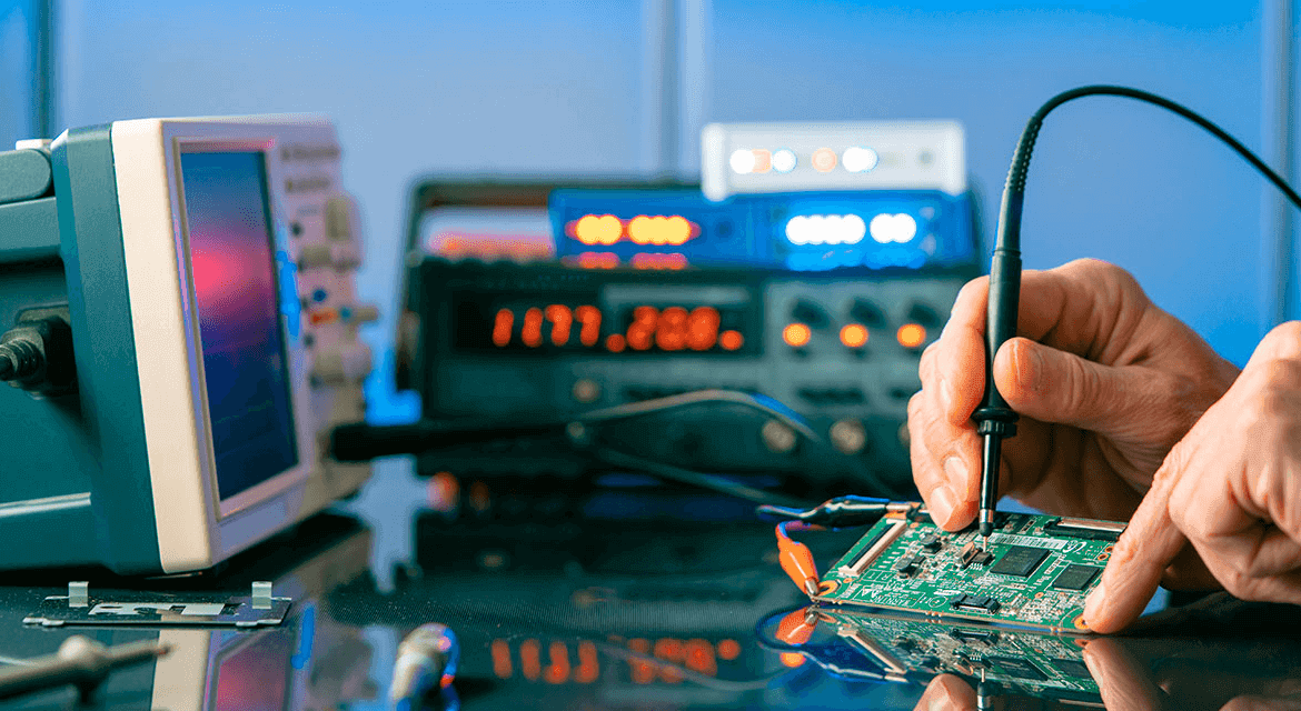
Flying Probe Testing: What It Catches and When to Use It Electrical test is the last chance to find a defect before a board leaves the factory, and it answers a question that no amount of visual inspection can. A board can look perfect and still have an open circuit,…
Hierarchical Design for Complex Schematics A schematic that fits on one sheet is easy to read and easy to review. A schematic that describes a system with a processor, two interfaces, a power supply and a dozen connectors does not, and the point at which a flat drawing stops working…
PCB Tented Via Rules: Covering a Via With Mask Modern electronics depend on boards that are assembled correctly the first time. Every product – a phone, a charger, a medical instrument or an industrial controller – relies on thousands of solder joints that must conduct current for years. This article…
PCB Sequential Lamination Steps: Building a Board in Stages Buyers and engineers often focus on the finished product and forget the production line behind it. In practice, most field failures can be traced back to process decisions made during assembly. Understanding PCB sequential lamination steps gives you a practical advantage…
PCB Via Filling Options: What Goes in the Hole Modern electronics depend on boards that are assembled correctly the first time. Every product – a phone, a charger, a medical instrument or an industrial controller – relies on thousands of solder joints that must conduct current for years. This article…
PCB Impedance Control on A Flex: Keeping the Number on a Bend Buyers and engineers often focus on the finished product and forget the production line behind it. In practice, most field failures can be traced back to process decisions made during assembly. Understanding PCB impedance control on a flex…