ENIG PCB Cost: Gold Thickness, Layers and Volume Electroless nickel immersion gold, known as ENIG, is the finish most engineers reach for when a board needs flat pads, long shelf life and a surface that survives multiple reflow cycles. It is also one of the more misunderstood items on a…

PCB Hole Tolerance for Press Fit: A Hole With No Room Modern electronics depend on boards that are assembled correctly the first time. Every product – a phone, a charger, a medical instrument or an industrial controller – relies on thousands of solder joints that must conduct current for years.…
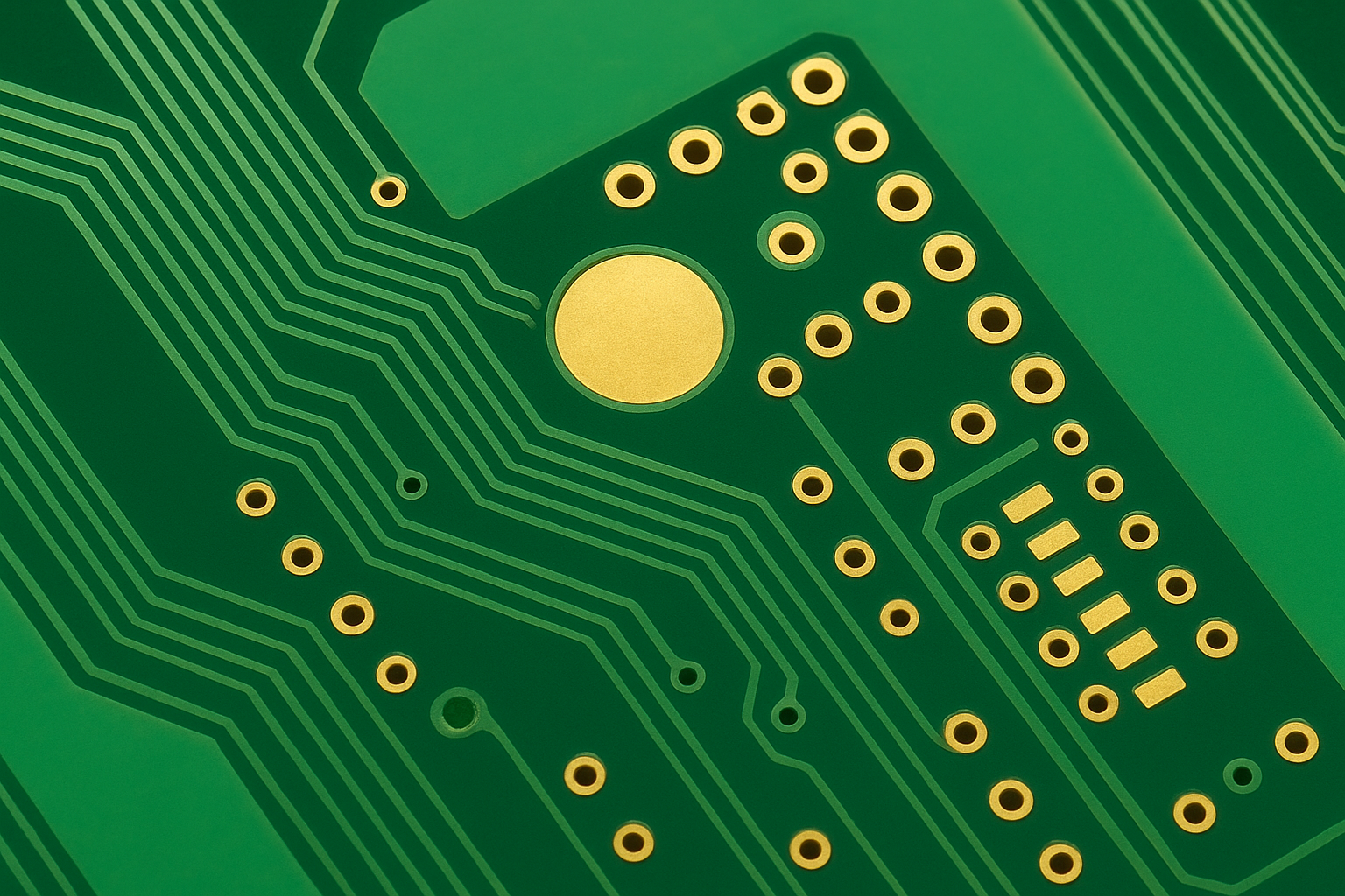
What Is on a Printed Circuit Board: Pads, Vias and Layers A printed circuit board is a set of copper features carried on an insulating base, organised so that a machine can place parts on it and solder them in one pass. Everything on the board belongs to one of…
Solder Mask Opening Over PCB Traces: When and How Most copper on a finished board is covered by solder mask, and that covering is assumed rather than designed. Occasionally a designer deliberately removes the mask over a trace, and the result is a solder mask opening that exposes bare copper.…
Reducing RF Effects in PCB Interconnect Design Below a few hundred megahertz a board can usually be treated as a set of ideal connections. Above that, the same copper begins to behave like a transmission line with delay, loss and coupling attached, and the layout decisions that were harmless at…
Blind Via PCB Manufacturing: Stackup, Process and Reliability A blind via is a hole that starts on an outer layer and stops at an inner layer instead of passing through the board. The idea is simple and the manufacturing is not: the hole has to be drilled to a controlled…
PCB Array Design for Assembly: Many Boards on One Panel Electronics manufacturing has become a discipline of small details. Solder paste volumes, placement accuracy, temperature profiles and inspection limits all add up to the final result. This guide looks at PCB array design for assembly from the perspective of a…
PCB Laser Depanelling: Cutting With Light Electronics manufacturing has become a discipline of small details. Solder paste volumes, placement accuracy, temperature profiles and inspection limits all add up to the final result. This guide looks at PCB laser depanelling from the perspective of a PCBA factory floor, covering cutting a…
PCB Thieving and Its Limits: Copper That Carries Nothing Buyers and engineers often focus on the finished product and forget the production line behind it. In practice, most field failures can be traced back to process decisions made during assembly. Understanding PCB thieving and its limits gives you a practical…
PCB Panel Bow and Twist: A Panel That Is Not Flat Modern electronics depend on boards that are assembled correctly the first time. Every product – a phone, a charger, a medical instrument or an industrial controller – relies on thousands of solder joints that must conduct current for years.…