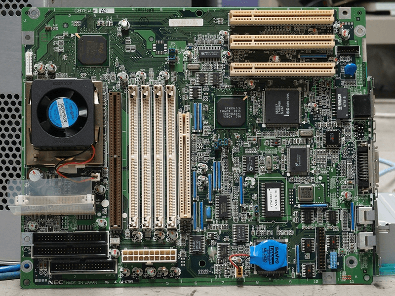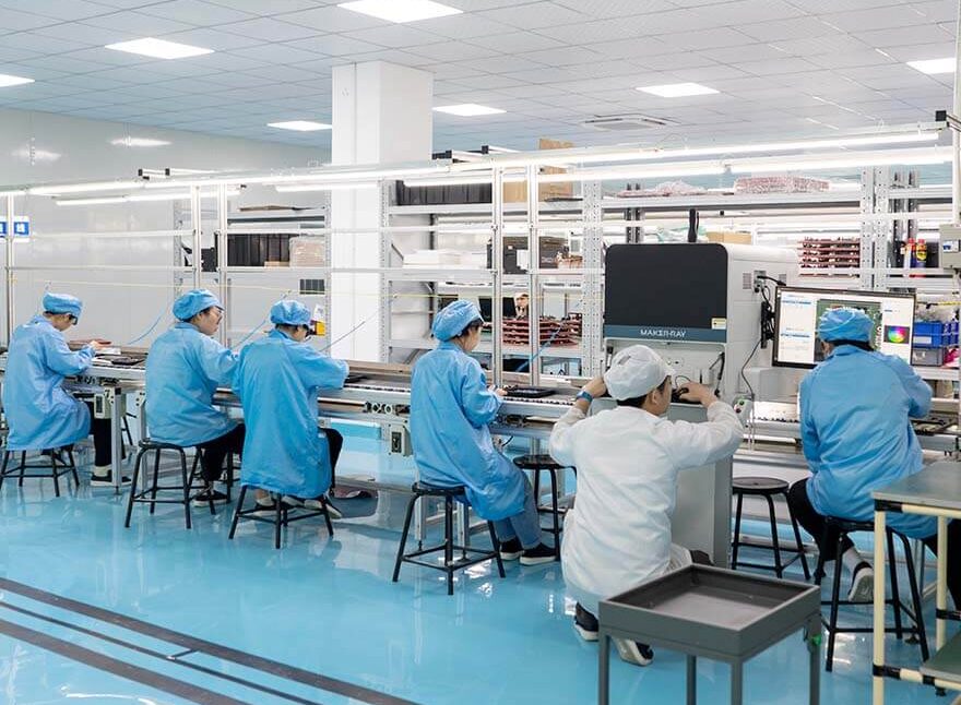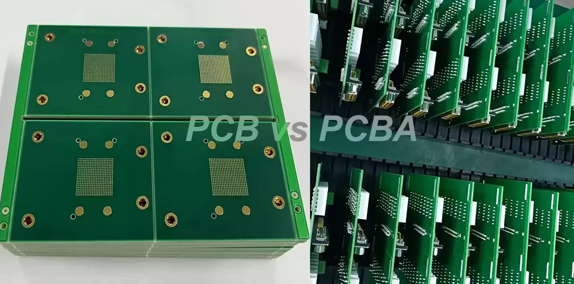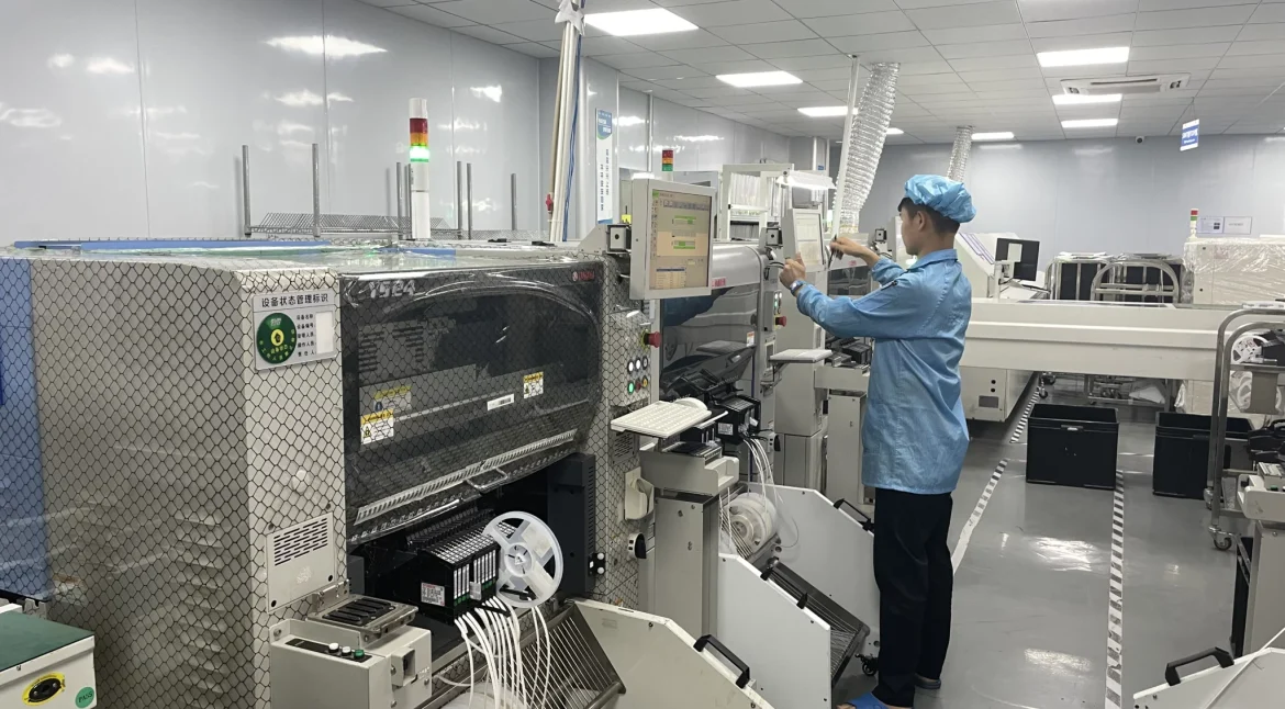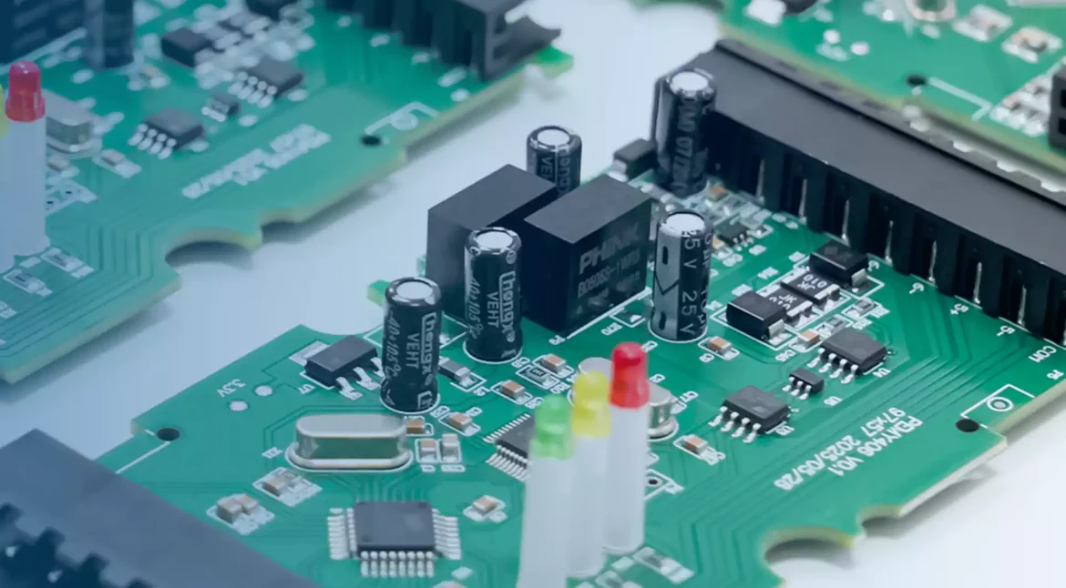
Automated Optical Inspection in PCB Manufacturing Inspection is the part of assembly that does not add value to the product, yet it decides whether the value produced upstream reaches the customer. Automated optical inspection has become the default way to check an assembled board because it is fast, consistent and…
Parallel PCB Design Flow for Dense High Speed Boards For a long time a printed circuit board could be designed in isolation. A circuit engineer finished a schematic, handed it over, and a layout engineer routed it before passing a data package to the fabricator. Each stage worked from the…
Copper Thickness and Via Plating in Multilayer PCB Fabrication A multilayer PCB is not a two layer board with more layers. The extra layers bring plated holes with a higher aspect ratio, inner layer copper that has to survive lamination, and impedance requirements that only hold if the whole process…
From Design Rules to DRC: A Practical PCB Workflow A layout tool will let a designer start drawing immediately, and that is the fastest way to produce a board that has to be reworked. The work that prevents rework happens in a fixed order at the beginning: the rules are…
Signal Integrity in the PCB Design Flow Signal integrity is not a property that can be added to a layout at the end. The decisions that decide it, which layer each signal runs on, what it is referenced to, and how far it runs beside its neighbours, are all taken…
ESP32 PCB Design: Layers, RF Layout and Antenna Clearance A board built around an ESP32 looks simple in the block diagram and behaves very differently in the layout. It carries a radio, a fast digital core and a switch mode supply on a board that is often smaller than a…
IoT PCB Copper Thickness: Choosing 0.5 oz or 2 oz Copper thickness is the parameter that quietly sets how much current a board can carry, how well it sheds heat and how much it costs, and on a small IoT board it is decided almost by accident. The designer chooses…
Standard 2-Layer PCB Thickness: 0.8, 1.0 and 1.6 mm Thickness is one of the first numbers a buyer fixes and one of the last to be reconsidered, even though it drives mechanical stiffness, thermal behaviour, impedance geometry and price at the same time. On a two layer board the choice…
PCB Manufacturing Defects: Causes and Prevention Every fabrication process has failure modes, and the useful thing about PCB manufacturing defects is that almost all of them are predictable. They cluster around a small number of physical mechanisms, they are visible under the right inspection, and they respond to specific process…
BGA Soldering: Voids, Reflow Profile and Inspection BGA soldering is the point at which the package stops being a part you can inspect with your eyes and becomes a set of joints you have to trust. The balls are underneath the body, the pitch is fine, and the process window…