Warpage and Fine Lines in an ABF Package Substrate A package substrate is the board that sits between a semiconductor die and the motherboard, translating a dense array of die pads into a coarser array of solder balls. As dies have grown larger and their connection counts have risen, the…
BGA Reballing: Stencils, Reflow Profile and Reliability Reballing is the process of removing the solder balls from a ball grid array package and attaching a new set. It is used to repair a package whose balls were damaged, to change the ball alloy when a product moves to a lead…
PCB Fabrication Notes: What to Send With Your Gerbers Most fabrication problems begin with a file that was complete in one respect and silent in another. The Gerber data describes the artwork, but it does not describe the material, the finish, the tolerance or the way the boards should be…
Copper Balance and Warpage in Multilayer PCB Lamination Warpage in a multilayer board is usually blamed on the press, and the press is often innocent. The board warps because the stresses built into it during lamination are unbalanced, and the most common source of imbalance is the distribution of copper.…
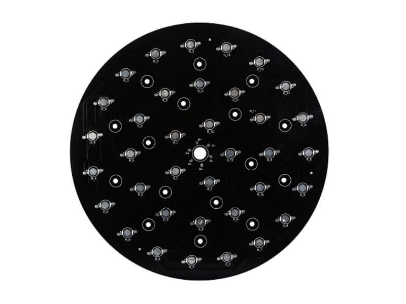
Metal Core PCB versus FR4: Thermal and Cost Comparison When a circuit generates more heat than an ordinary laminate can remove, the first question is whether the problem is really thermal or whether it is a matter of layout. A metal core PCB solves a specific problem: it spreads heat…
Gold Fingers and Edge Connector Design A gold finger is a row of equally spaced rectangular pads along the edge of a board, plated with gold and left free of solder mask. The board slides into a slot connector and the pads make contact with the spring contacts inside it,…
PCB Panelization: Why Boards Are Combined A small board is difficult to manufacture and even more difficult to assemble. It does not fit the fixture, it does not feed through the placement machine reliably, and it wastes panel area if it is produced one at a time. PCB panelization is…
PCB Prototype Order: Every Field You Must Specify A PCB prototype order is a specification, and the fabricator will build exactly what the specification says rather than what the designer intended. Every field that is left blank is filled in with a default, and the default is chosen for cost…
PCB Touch Sensor Overlay: The Panel in Front Buyers and engineers often focus on the finished product and forget the production line behind it. In practice, most field failures can be traced back to process decisions made during assembly. Understanding PCB touch sensor overlay gives you a practical advantage when…
PCB Hall Sensor Placement: Where the Field Is Strongest Electronics manufacturing has become a discipline of small details. Solder paste volumes, placement accuracy, temperature profiles and inspection limits all add up to the final result. This guide looks at PCB hall sensor placement from the perspective of a PCBA factory…