PCB LED ESD Damage: A Dark Spot on the Line Electronics manufacturing has become a discipline of small details. Solder paste volumes, placement accuracy, temperature profiles and inspection limits all add up to the final result. This guide looks at PCB LED ESD damage from the perspective of a PCBA…
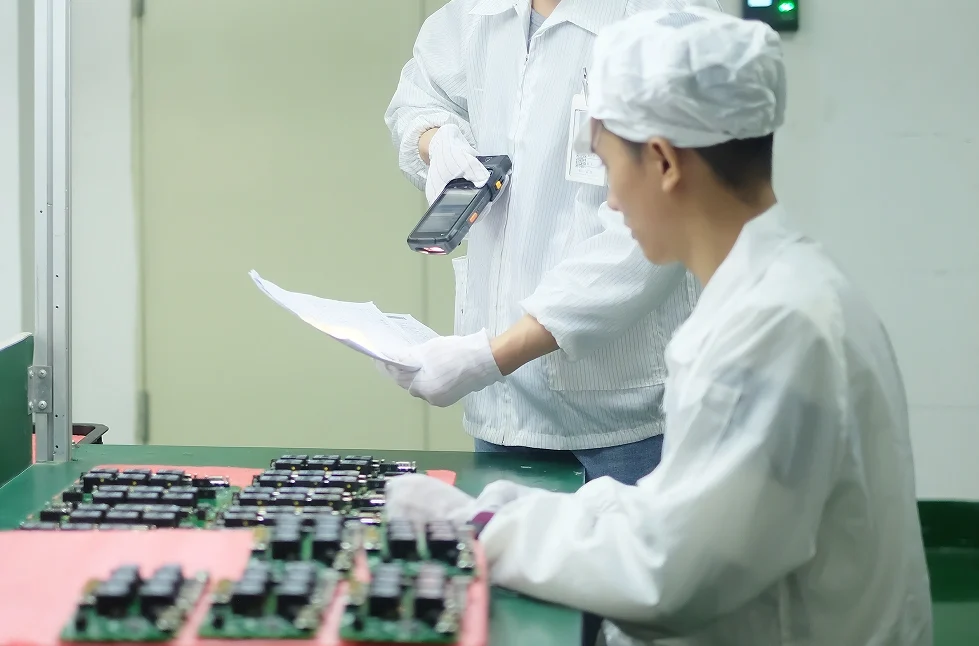
PCB Sensor Calibration on Board: Trimming in Place Electronics manufacturing has become a discipline of small details. Solder paste volumes, placement accuracy, temperature profiles and inspection limits all add up to the final result. This guide looks at PCB sensor calibration on board from the perspective of a PCBA factory…
PCB Silkscreen Design: Line Width, Clearance and Marking Silkscreen is the layer of the design that people read. It identifies the components, marks the orientation of the parts that can be fitted the wrong way, warns about handling restrictions and carries the identifiers that link a board to its documentation.…
PCB Trace Width and Current: How to Size Conductors Sizing a conductor is one of the few calculations in board design that can be done on the back of an envelope, and one of the few that is routinely done badly. The physics is simple: a trace has a cross-sectional…
PCB Reverse Engineering: How the Process Actually Works Reverse engineering a board starts from the finished object and works backwards to a schematic. It is used to document equipment that has no available drawings, to reproduce a board whose manufacturer no longer supports it, and to understand how a competitor…
Solder Mask and Paste Mask: Openings, Dams and Stencil Two layers in a circuit board drawing are routinely confused. The solder mask is the permanent coating on the finished board, and the paste mask is a drawing of the openings in the stencil that deposits solder paste during assembly. They…
PCB Board Thickness: Standard Values and Tolerances Board thickness looks like the simplest parameter in a fabrication drawing and it is one of the most frequently misunderstood. A nominal figure such as 1.6 mm describes a finished board, including the copper and the plating, and the laminate that is ordered…
Plated Slot vs Non-Plated Slot in PCB Design Not every hole in a board is round, and not every elongated opening is meant to carry current. A slot can be metallised so that it connects layers and carries a heavy current, or left as bare laminate so that it only…
PCB Warpage: Bow, Twist and Stackup Balance Warpage is the permanent deformation of a board that should be flat. It appears as a bow along one axis, as a twist across the diagonal, or as a local hump over a copper heavy area, and it shows up at the worst…
PCB RTD Wiring: Three Wires or Four Electronics manufacturing has become a discipline of small details. Solder paste volumes, placement accuracy, temperature profiles and inspection limits all add up to the final result. This guide looks at PCB RTD wiring from the perspective of a PCBA factory floor, covering wiring…