PCB Capture Pad Design: Annular Ring, Registration and Reliability A capture pad is the copper area that surrounds a drilled hole on the layer where the via begins or ends. It exists for two reasons: to guarantee that the hole lands inside copper despite registration and drill tolerance, and to…
PCB Cooling Zone in Reflow: Slowing the Fall Modern electronics depend on boards that are assembled correctly the first time. Every product – a phone, a charger, a medical instrument or an industrial controller – relies on thousands of solder joints that must conduct current for years. This article explains…
Running a Pre-Release PCB Design Review Most board re-spins are not caused by a clever circuit that did not work. They are caused by a footprint with the wrong pad spacing, a connector placed too close to its neighbour, a silkscreen reference sitting on top of a via, or a…
Medical Electronics PCB: Applications and Requirements Medical electronics is a broad category that ranges from a disposable glucose strip to a surgical robot, and the boards inside them have little in common except the regulatory framework they sit in. What distinguishes a medical PCB is not usually the circuit but…
PCB Solder Paste Volume Per Joint: How Much Paste a Joint Needs Electronics manufacturing has become a discipline of small details. Solder paste volumes, placement accuracy, temperature profiles and inspection limits all add up to the final result. This guide looks at PCB solder paste volume per joint from the…
Power Plane Design: Current Capacity and Splitting Power distribution is the part of a layout that is easiest to defer and most expensive to get wrong. It is not a single net with a single rule; it is a set of copper shapes, via arrays and plane boundaries that have…
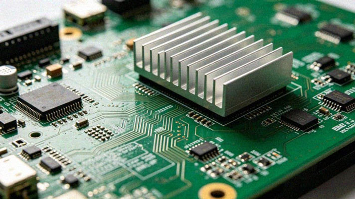
Embedded Copper Coins: How Heat Leaves a Board Coin insertion, also called embedded copper, is the practice of pressing a solid piece of copper into a cavity in the board so that its face is flush with the surface. The coin becomes part of the thermal path, and in some…
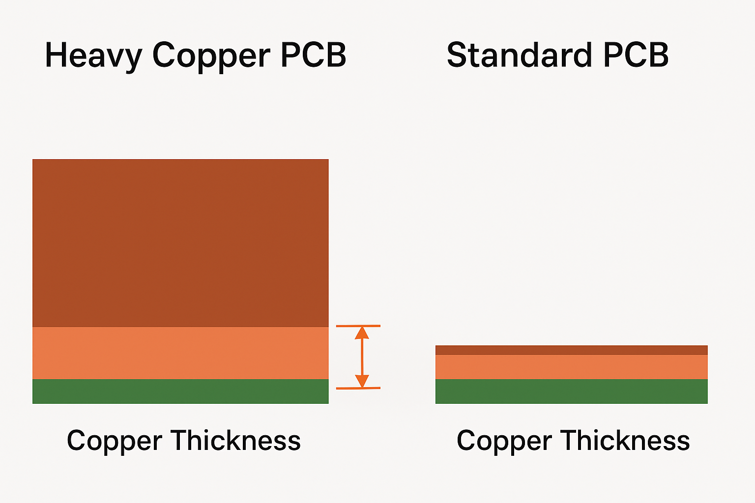
PCB Dimensions: Thickness, Tolerances and Edge Clearance PCB dimensions are the set of mechanical parameters that decide whether a board can be built, assembled and fitted into its enclosure: length and width, thickness, copper weight, hole size, outline tolerance and the clearance between the outermost copper and the board edge.…
PCB Hole Structures: Blind Via, Buried Via and Microvia The holes in a circuit board are not all the same thing, and the differences between them determine how dense a design can be, how much it costs and how reliable it turns out. A through hole that accepts a component…
Additive PCB Manufacturing: Process, Advantages and Limits Almost every circuit board in production today is made by subtraction. A panel arrives covered in copper, a resist protects the pattern, and the unwanted metal is etched away. Additive PCB manufacturing turns that logic around: copper is deposited only where the circuit…