PCB Design Practice: Board Size and Device Placement
Practitioners accumulate rules that are not written in any standard, and the two that matter most concern the physical extent of the board and the arrangement of the devices on it. Both are decided early, both are difficult to change later, and both have effects that appear as noise rather than as an obvious fault.
Board Size Is an Electrical Decision
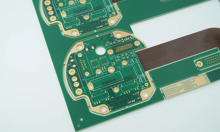
Making a board larger lengthens every connection, and a longer connection has more resistance and more inductance. In digital circuits that added impedance reduces the noise margin and slows the edges; in analog circuits it makes the reference less stable and the measurements noisier. The cost rises as well, because the board area is the primary driver of the price.
Making the board smaller has its own penalties. A compact board concentrates heat, so components that dissipate power run hotter and their lifetime shortens. It also places the traces closer together, which increases the coupling between them and makes the layout more sensitive to any interference from a nearby conductor. A board that is too small can also suffer from mechanical problems, because the copper density is high and the stiffness of the laminate is reduced.
The practical approach is to size the board from the mechanical envelope and the component count, then to check the two extremes. Where the layout must be dense, the extra care goes into separation and reference continuity; where it can be generous, the extra area should be used for ground and for spacing rather than spread evenly across the design.
Grouping Devices That Belong Together
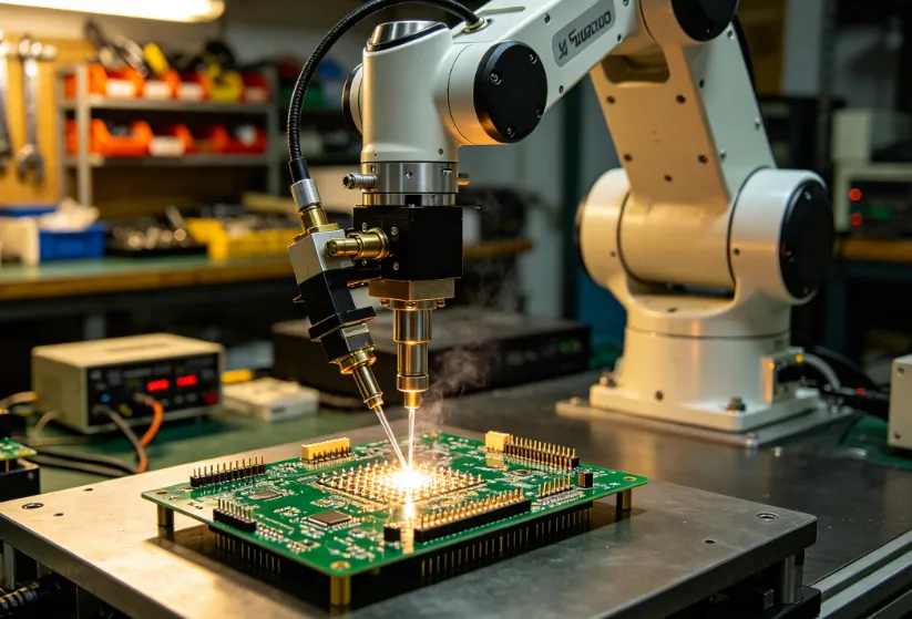
The placement rule that produces the largest benefit is grouping. Devices that are logically related should be physically close, because the connections between them are the ones that carry the critical signals. A clock generator, a crystal and the clock input of a processor form a group that should be as compact as the layout allows, since every millimetre of trace between them adds jitter and picks up noise.
The same principle applies to the supply. A regulator, its input and output capacitors, its inductor and its load form a group that has to be tight for the current loop to stay small. Splitting that group across the board is the most common reason a converter that simulated perfectly produces more ripple than expected.
Grouping is also what makes the return paths short. When related devices sit together, the return current for their signals flows over a small area of the ground plane, and the loop that could radiate is correspondingly small. The geometry of that return path is the subject of this article on ground routing and power trace planning.
Separating the Noise Sources
Devices that generate noise and circuits that are sensitive to it should be as far apart as the board allows. Clock generators, switching regulators, motor drives, relays and any circuit that switches a large current belong in that first category. Low-level analog inputs, sensor conditioning chains, reference circuits and high-impedance nodes belong in the second.
Where the separation cannot be achieved by distance alone, the alternatives are a change of layer, a ground plane between the two regions, or a shield. All three work by interrupting the coupling path rather than by reducing the source, which is why they are more reliable than attempting to filter the noise after it has already reached the sensitive circuit. Where the design includes a high-current section and a low-level measurement section, splitting them onto separate boards is sometimes the correct answer, and it is worth considering before the layout rather than after.
Current Loops and Where They Close
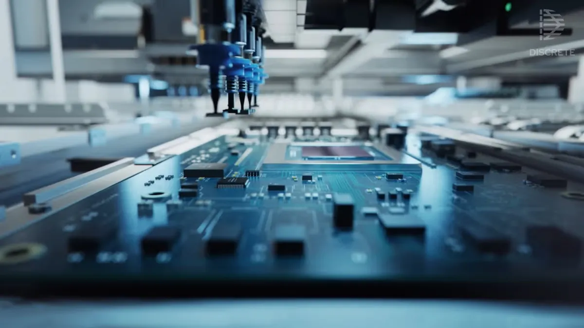
Every signal and every supply connection forms a loop with its return, and the area of that loop determines how much the circuit radiates and how susceptible it is to external fields. Placement decides the loop area before routing begins, because the distance between a device and its decoupling capacitor, or between an output stage and its load connection, is a placement decision rather than a routing one.
The general rule is that a loop should be as small as the function allows. The decoupling capacitor belongs at the pin, the series termination belongs at the driver, and the return connection for a high-current output should run beside the outgoing conductor rather than through the general ground plane. Each of those arrangements shortens the loop, and each is fixed at placement time.
The measurement of the current itself is a useful check. Where a design includes a shunt resistor for current sensing, its position determines which parts of the circuit share a ground return with the measured current, and a poorly chosen position produces a measurement that includes the voltage drop of unrelated currents. This is the same class of problem described in the discussion of trace width and current calculation.
Reference Planes and the Order of Placement
Placement should also respect the reference arrangement. On a board with a continuous ground plane, the devices should be arranged so that their return currents do not have to cross the paths of other return currents. Where the board has separate analog and digital regions, the boundary between them should follow the signal flow, so that the converters that straddle the two domains sit on the boundary rather than in the middle of one domain.
The order of placement that keeps these constraints satisfiable is mechanical parts, then the core device, then the power section, then the clock and analog groups, then the interfaces and finally the passives. Placing in that order means each decision is made with the constraints already known, and it avoids the common situation where a designer discovers halfway through that the crystal cannot be placed where the layout requires it.
Reviewing the Placement
Before routing begins, it is worth reviewing the placement against four questions. Are the critical signals short? Are the noise sources separated from the sensitive circuits? Is every decoupling capacitor adjacent to the pin it serves? And does the current loop of the highest-current path stay within the area intended for it? A placement that answers those four questions well will usually route easily, and a placement that does not will consume the routing time that was saved by not checking.
Practices That Save Time Later
Two habits repay their cost on almost every design. The first is to keep the schematic current while the layout is in progress, so that a change is reflected in both representations at the same time rather than accumulated into a revision that has to be reconciled later. The second is to record the reasoning behind unusual geometry, because a trace that takes an odd path will be re-routed by the next engineer unless the constraint that forced it is documented. Both habits are free, and both prevent the situation where a design cannot be modified because nobody knows why it was built that way. The dimensional and clearance rules that such records usually reference are set out in this discussion of via to trace clearance.
FAQ
Does a larger board reduce noise? Not automatically. A larger board reduces the density of the traces and gives more room for ground, which helps, but it also lengthens every connection and increases the loop area for signals that must travel across it. The benefit comes from using the extra area well, not from the size itself.
How far apart should noise sources and sensitive circuits be? As far as the board allows, and ideally in different regions with a different reference arrangement. Where distance is not available, a change of layer with a ground plane between, or a shield, is more reliable than trying to filter the interference once it has arrived.
Why does device grouping matter so much? Because it determines the length of the critical connections and the size of the return loops before any routing is done. Grouped devices have short signal paths and small return loops, while the same components scattered across a board produce longer paths and larger loops that no routing technique can correct.