Brain Computer Interface PCB: Capturing Microvolt Signals at 64 Channels
A brain computer interface PCB works at the edge of what electronics can resolve. Cortical signals arrive in the microvolt range, several orders of magnitude below the noise that ordinary digital circuitry generates, and the acquisition board has to deliver those signals to an analogue to digital converter without distorting them.
A recent 64 channel acquisition programme illustrates the difficulty. Two earlier suppliers produced samples at roughly sixty percent yield and could not close electromagnetic compatibility testing, which is what happens when a board treats biological signals as an ordinary analogue input.
What the Signal Actually Looks Like
Cortical recordings span a few microvolts to a few hundred, with useful content concentrated below a few hundred hertz. That bandwidth is narrow, which helps filtering, but the amplitude is the problem.
The reference point matters as much as the measurement. A signal chain that resolves a microvolt must also reject common mode interference, electrode offset and drift, all of which are far larger than the signal being captured.
Why Sixty Four Channels Change the Problem
One channel can be routed carefully by hand. Sixty four channels drawn in parallel across a small board create coupling paths between neighbours, and crosstalk that is negligible on a single trace becomes a systematic error across an array.
Targets for such a design are demanding: sensitivity in the microvolt range, signal to noise ratio above eighty decibels, and channel to channel crosstalk held below minus sixty decibels while microvolt signals travel beside digital clocks switching at megahertz rates.
The Architecture of an Acquisition Board
A complete board integrates four functions that want different things from the same substrate. An analogue front end conditions and amplifies the electrodes, converters digitise the result, a digital section processes it, and a wireless link transmits the data.
Each block has its own noise signature. The analogue front end wants quiet ground and shielding, the digital section radiates switching noise, and the radio link adds bursts of current at unpredictable moments. Layout decides whether they coexist or interfere.
Shielding and Isolation at Three by Three
Running sixty four channels in a small area forces extremely fine geometry, with trace width and spacing around three thousandths of an inch. At that pitch, a small routing deviation or a layer to layer coupling path injects noise directly into the measurement.
Conventional film exposure struggles to hold the required accuracy at that geometry. Laser direct imaging removes the film alignment error and holds line width within a fraction of a thousandth of an inch, which is what makes the isolation between adjacent channels repeatable. Production at that scale belongs to PCB manufacturing processes built for fine line work rather than adapted to it.
Ground Strategy and Reference Planes
Splitting analogue and digital ground into separate regions and joining them at a single point is a standard recommendation that becomes essential at these amplitudes. Multiple return paths create loops that carry digital current through the analogue reference.
Adding ground traces between critical signal lines, keeping the analogue plane continuous beneath the front end, and separating sensitive inputs from clock routing are the measures that keep the reference stable when the digital section is active.
Rigid Flex Construction for Wearable Variants
Non invasive versions of these systems are worn on the head, so the acquisition electronics cannot sit on a single flat board. A ten layer high density rigid flex structure allows the sensing array and the processing section to be joined without connectors.
The transition between rigid and flexible sections is where impedance changes abruptly. Differential pairs crossing that boundary need compensated geometry and simulated verification, or reflections appear at exactly the point where the signal leaves the sensing region.
Impedance Targets in a Moving Structure
Differential channels in these designs are often specified at one hundred ohms with a five percent window. Holding that across a rigid flex transition requires the flex section stackup to be designed as part of the same impedance model.
Coverlay openings, stiffener placement and bend location all affect the result. When the design is reviewed before release, impedance discontinuities can be reduced substantially; when they are discovered during validation, the correction usually requires a new tooling cycle.
Implantable Format and Extreme Miniaturisation
Implantable variants compress the same functionality into roughly thirty by twenty millimetres. At that size every millimetre of board area carries an electrical cost, and layer count rises because there is no space to spread out.
Higher performance laminate grades with stable dielectric properties support thinner dielectrics and finer lines at those dimensions. The material choice is driven as much by dimensional stability during lamination as by electrical loss.
Clock Distribution and Sampling Accuracy
Sixty four converters sampling simultaneously need a clock that arrives at every device within a controlled window, typically tighter than fifty picoseconds. That requirement turns clock routing into the most constrained net on the board.
Matched lengths, controlled via stub lengths and continuous reference planes all contribute. A single discontinuity shifts arrival time at one converter, and the resulting sampling offset degrades a measurement that no downstream processing can recover.
Impedance Verification on Every Unit
Measuring a sample board is not sufficient when the process window is this narrow. Testing every unit for impedance and applying time domain reflectometry to critical differential pairs locates anomalies that a pass or fail test alone would miss.
In the programme described here, differential impedance pass rate moved from the low eighties to one hundred percent, and measured skew settled near thirty eight picoseconds against a fifty picosecond limit. Those numbers come from measurement discipline rather than from design intent.
Medical Grade EMC Compliance
Devices that connect to a patient fall under IEC 60601-1, which constrains emissions, immunity and patient leakage current. Sensitivity and emissions pull the layout in opposite directions, because shielding and filtering add capacitance and reduce usable bandwidth.
The practical resolution is separation. Physically dividing fast digital regions from analogue sensing regions, controlling the return path of every switching current, and keeping the patient connected section small limits both what the board emits and what reaches the electrodes.
Four Stage Quality Control
Incoming inspection, solder paste measurement, three dimensional optical inspection and X-ray review of hidden joints form a sequence, and functional testing at the end confirms behaviour rather than appearance.
Each stage catches a different failure mode. X-ray finds voids and bridges beneath packages that optical inspection cannot see, while functional test at the specified sensitivity reveals marginal analog channels that pass continuity checks but fail in use. A quality management system is what keeps those stages consistent across lots.
Design Review Before Fabrication
Most of the difficulty in these programmes is decided before the first panel is made. Front end design review examines analogue routing, ground partitioning, the rigid flex transition and coverlay openings while changes are still inexpensive.
Teams that perform that review as a joint exercise with fabrication and assembly often reduce the number of tooling iterations, because impedance and manufacturability problems are corrected on paper rather than in copper.
Assembly of Fine Pitch Mixed Technology
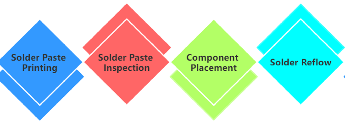
An acquisition board mixes analogue front end packages, fine pitch converters, a processor and a radio module on one surface. Paste volume control matters more than usual, because an analogue input with marginal solder coverage produces intermittent noise rather than an obvious defect.
Support fixtures and controlled profiles keep placement stable, and the assembly step is best treated as part of the same process chain as fabrication. This is where medical PCBA experience with low volume, high mix builds becomes relevant.
Yield, Iteration and the Path to Production
Moving from sixty two percent to more than ninety six percent yield took three engineering iterations, and the improvements came from systematic causes: registration, grounding, impedance consistency and inspection coverage.
Speed helps, but only when it is paired with evidence. A programme that goes from samples to volume production in about twenty five days is usually one where the process parameters were already understood before the ramp began.
What Clinical Use Will Demand Next
Channel counts will continue to rise, and implanted systems will add hermetic sealing, long term material compatibility and stimulation circuitry alongside recording. Each addition raises density and lowers the tolerable noise floor.
Manufacturing will have to follow, with finer lines, more layers and tighter impedance control in parts that are physically smaller. For suppliers, the durable advantage is not a single capability but the ability to reproduce a demanding build repeatedly, which is the essence of PCBA capability at this level.
Choosing a Partner for Neural Hardware
Questions worth asking are specific to the application: how fine a line the process holds in production, how impedance is verified per unit, how rigid flex transitions are simulated, and what cleanliness controls apply to sensitive analogue assembly.
Answers should come with records rather than assurances. Neural signal acquisition is unforgiving of small process variation, and the supplier who can show measured data is the one likely to deliver consistent boards.