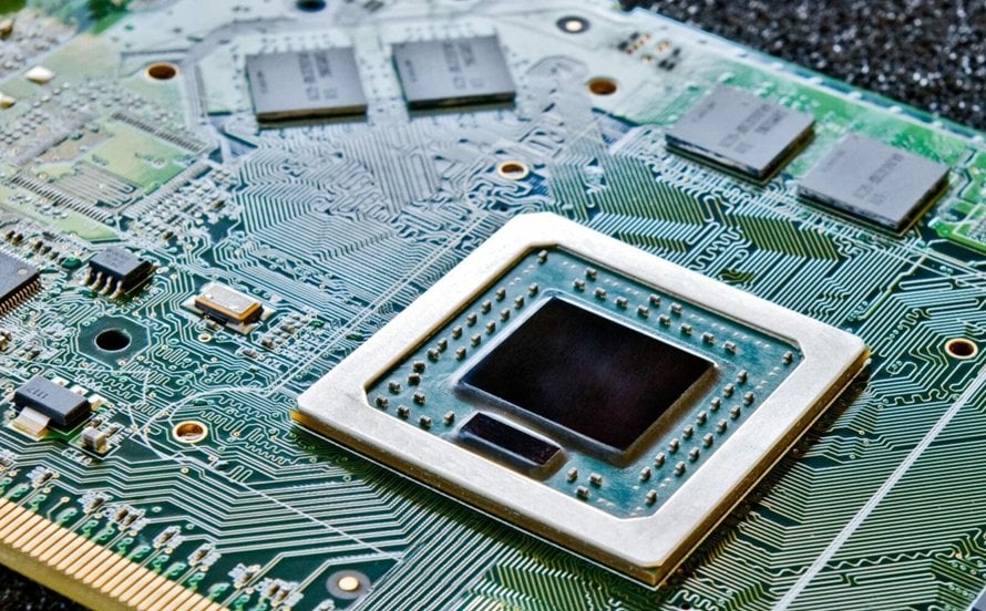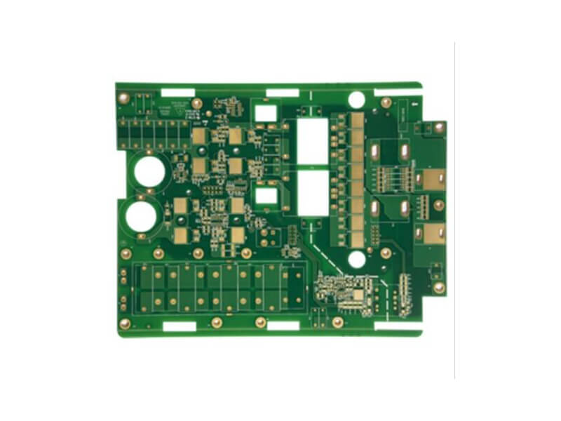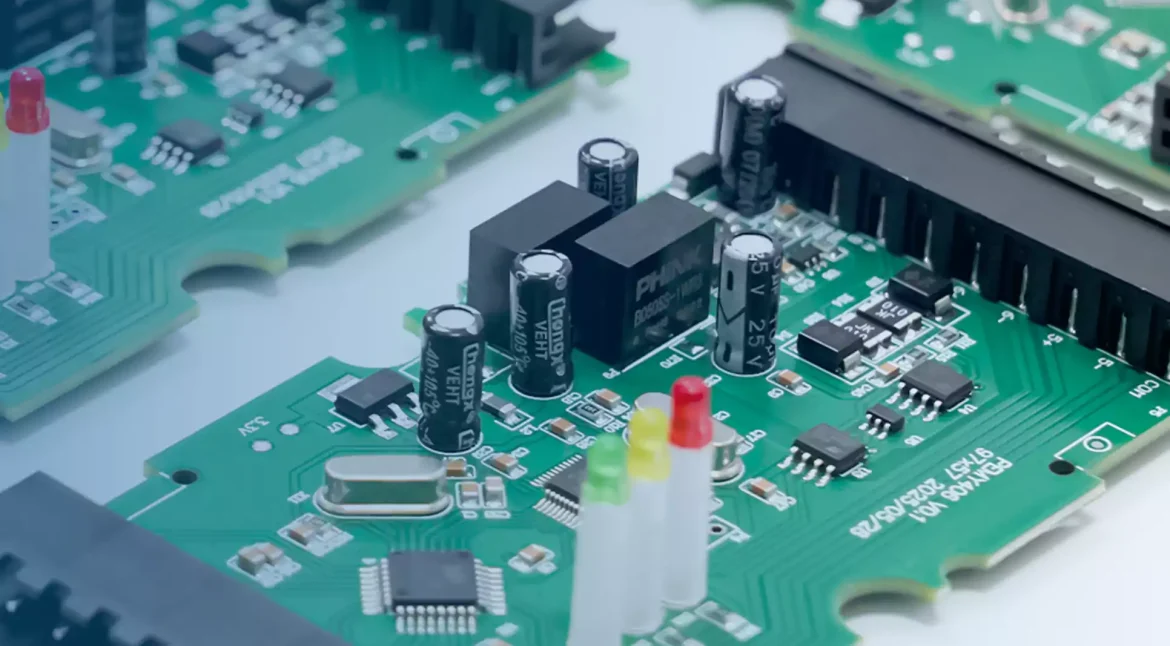


Burn-In and Aging Tests for Assemblies What an Aging Test Screens Every population of manufactured assemblies contains a small number of units with a latent defect that will fail early. The distribution of failures over time follows a curve with three regions: a decreasing failure rate at the start, caused…
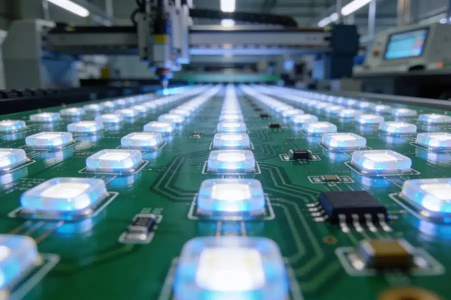
Incoming Inspection of Bare Boards Why Inspect on Receipt An incoming inspection is the last opportunity to reject a board before value is added to it. Once components are placed and reflowed, a fault that came from the bare board is indistinguishable from an assembly fault until a considerable amount…
SMT Component Reel Change: Loading a Fresh Reel Modern electronics depend on boards that are assembled correctly the first time. Every product – a phone, a charger, a medical instrument or an industrial controller – relies on thousands of solder joints that must conduct current for years. This article explains…
Board Edge Clearance Rules Explained Why the Edge Needs Clearance The outline of a board is produced by routing, scoring or punching, and each of those operations has a tolerance and a mechanical effect on the material near the cut. Copper that reaches the edge can be torn, exposed, shorted…
Cold Solder Joints: Causes and Detection What a Cold Joint Is A cold joint is one in which the alloy did not fully melt, or did not form a proper metallurgical bond with the surfaces, so the joint is mechanically and electrically inferior despite appearing connected. The classic visual signature…
PCB Via Aspect Ratio: The Depth to Width Modern electronics depend on boards that are assembled correctly the first time. Every product – a phone, a charger, a medical instrument or an industrial controller – relies on thousands of solder joints that must conduct current for years. This article explains…
Heavy Copper PCB: Etching and Plating Limits What Counts as Heavy Copper Heavy copper usually means a layer of three ounces per square foot or more, which is roughly 105 micrometres, and the term extends to boards with copper an order of magnitude thicker for high current applications. The distinction…
SMT Reflow Solder Paste Transfer Efficiency: How Much Paste Lands Buyers and engineers often focus on the finished product and forget the production line behind it. In practice, most field failures can be traced back to process decisions made during assembly. Understanding SMT reflow solder paste transfer efficiency gives you…
PCB Antennas: Clearance and Layout Rules How a PCB Antenna Works A printed antenna is a copper pattern whose dimensions and surroundings set its resonant frequency and its impedance. Because it is etched on the same board as the rest of the circuit, its performance depends on things that would…
PCB Copper Trace Manufacturing Tolerance: Staying Inside the Limit Electronics manufacturing has become a discipline of small details. Solder paste volumes, placement accuracy, temperature profiles and inspection limits all add up to the final result. This guide looks at PCB copper trace manufacturing tolerance from the perspective of a PCBA…