
Why The Board Came Back At The Wrong Characteristic Impedance
A designer calculates a trace width for fifty ohms, sends the Gerber files out, and receives boards that measure a few ohms away from the target. Nothing in the design changed, and yet the number moved. The reason is that the calculation produced a width for a set of material assumptions, and the board was built from materials that did not match those assumptions exactly.
This article explains where the difference comes from, which variables drive it, and what can be put on the fabrication drawing so that the characteristic impedance that comes back is closer to the one that was designed.
Understanding the cause is worthwhile because most of the gap is predictable, and a predictable gap can be negotiated with the fabricator rather than discovered on a test bench.
The Laminate Is Not The Datasheet
The dielectric constant of FR-4 is quoted as a range rather than a value, and the range is wide. Material sold as the same grade can arrive with a dielectric constant anywhere from the high threes to the high fours depending on the resin content and the supplier, and a half point of difference is enough to move a fifty ohm microstrip by several ohms. The datasheet value is a nominal figure for a family of materials, not a measurement of the lot in the crate.
The effect is larger at high frequency, where the field spends more of its time in the dielectric. This is why a laminate intended for RF work is specified with a tolerance on the dielectric constant as well as a nominal value; the consistency of the material is what makes the impedance repeatable, not merely the nominal figure.

Thickness, Copper And The Trapezoid
The dielectric thickness between a trace and its reference plane is set by the laminator, and it carries a tolerance of its own. A thicker dielectric raises the impedance of a microstrip, and a thinner one lowers it. On thin boards the contribution of the prepreg sheets becomes significant, and a change of one sheet changes the result. After pressing, the only way to know what was actually built is to section a sample and measure it.
Copper thickness is the second variable, and it also carries a tolerance. A heavier foil makes the conductor wider in effect and lowers the impedance, and the plating added afterwards changes it again. The etch process adds a third contribution: etchant attacks the copper from both sides, so the finished trace is narrower at the bottom than at the top. The result is a trapezoidal cross section whose effective width is less than the top width, and the size of that effect is described by the etch factor of the process. It matters most on narrow traces, which is exactly where the tightest tolerances are needed.
Reflow And Storage Change Things Too
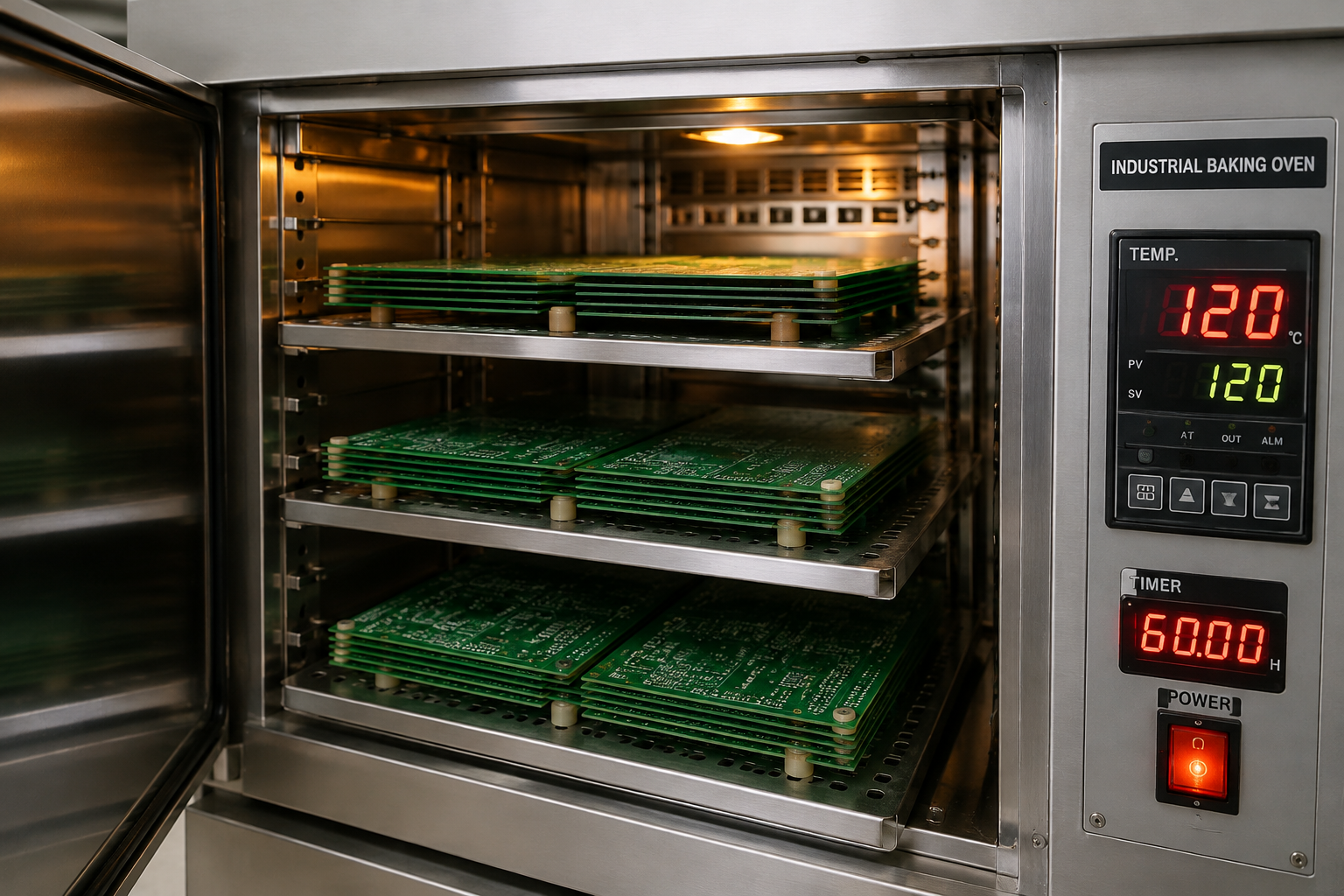
A board that has been through reflow is not the same board that was measured at the fabricator. Heat and moisture uptake shift the dielectric properties of the laminate, and thermal expansion moves the geometry slightly. A coupon measured before assembly can therefore disagree with an assembled product, and the disagreement is systematic rather than random.
The practical consequence is that the coupon should be measured under conditions that represent the finished article where the application is sensitive, or the expected shift should be allowed for in the tolerance. Boards that have absorbed moisture in storage also measure differently, which is one reason a controlled impedance specification is easier to meet on a shop that controls the environment than on one that does not.
What Belongs On The Drawing
The first improvement is to stop writing FR-4 as if it were a specification. Naming the laminate family, and where possible the exact grade and its dielectric constant tolerance, gives the fabricator something to buy against and something to check on receipt. For RF work, a laminate with a tight dielectric constant specification is worth the premium if the impedance really has to be held.
The second is to state the impedance target and the tolerance, per layer, with the reference plane identified. A note that says fifty ohms on the top layer over the ground plane, plus or minus five percent, is actionable. A note that says controlled impedance, without a number, is not. The third is to ask the fabricator to recalculate the line width for the material they will actually use and to send that calculation back before the panel is released, which is what an experienced shop does by default when the artwork is reviewed at CAM.
Verifying The Finished Board
Measurement is the other half of the loop. A time domain reflectometer reading of the finished board, compared against the design value, turns the discussion from an opinion into data. If the board is consistently low, the fabricator can compensate by narrowing the trace; if it is consistently high, the compensation goes the other way.
Where a product will be built in volume, it is worth treating the first panel as a measurement exercise. Building a prototype panel to the intended stackup, measuring it, and then adjusting the artwork before the production order costs one extra iteration and removes the risk of a whole batch that misses. The alternative, discovering the error after assembly, costs considerably more.
Working With The Shop On The Number
Some of the gap between calculated and measured impedance cannot be removed, but almost all of it can be managed. Choose a laminate whose dielectric constant is specified rather than implied. Give the fabricator the target and the tolerance. Ask for the width to be recalculated against the real material. Measure the finished board and feed the result back. Each of those steps is cheap, and together they move the result from a rough approximation toward a controlled value.
It helps to remember that the calculation is only half of the model. The geometry comes from the design, and the electrical behaviour comes from the material, and the material belongs to the fabricator. The design rule worth adopting is to specify the target, not the width, and to let the shop that will build the board decide how to reach it. gopcb works with customers on that basis, recalculating line widths against verified material data and confirming the result with a measurement on the finished panel. The same discipline applies when a design follows manufacturable design guidelines, because the tolerance that matters is the one the process can hold.
FAQ
Why does the same trace width give different impedance at two board houses? Because their copper thickness, dielectric thickness, etch behaviour and solder mask differ. The width has to be calculated for the shop that will build the board.
Can the impedance be corrected after the first lot? Yes, by adjusting the artwork width in the compensation. That is the normal way a controlled impedance relationship settles down.
Is a high frequency laminate always necessary? No. It is necessary when the dielectric constant tolerance and the loss of FR-4 are not good enough for the specification. Where they are, FR-4 with a known lot value will do.