Understanding COB Packaging on HDI PCB and PCB Proofing Requirements
Modern electronic products continue to demand smaller sizes, higher performance, and improved reliability. To achieve compact designs with excellent electrical performance, manufacturers increasingly use advanced technologies such as HDI PCB, miniaturized components, and innovative chip packaging solutions.
One important technology used in compact electronic devices is COB Packaging (Chip on Board Packaging). This method directly mounts bare semiconductor chips onto a printed circuit board, helping reduce space requirements while improving product integration.
For companies developing new electronic products, professional PCB Proofing is also an essential step before mass production. Prototype testing helps verify circuit performance, component compatibility, and manufacturing feasibility.
Through advanced PCB Manufacturing capabilities and reliable PCB Assembly processes, manufacturers can support customers from initial prototype development to large-scale production.
For more information about professional circuit board solutions, visit our PCB Manufacturing Service.
What Is COB Packaging Technology?
COB stands for Chip On Board, which is a direct chip mounting technology where semiconductor dies are attached directly onto the surface of a PCB.
Unlike traditional packaged IC components, COB technology eliminates some external packaging structures. The bare chip is positioned on the circuit board, electrically connected through bonding wires, and then protected with epoxy resin or other encapsulation materials.
The black epoxy-covered area commonly seen on some circuit boards is usually the protective layer of the COB process. It protects the internal chip and bonding wires from environmental damage, vibration, and mechanical stress.
The basic COB packaging process includes:
1. Chip Placement
The semiconductor chip is accurately positioned on the PCB surface using automated equipment to ensure alignment accuracy.
2. Wire Bonding
Fine metal wires connect the chip electrodes with PCB pads, creating electrical connections between the IC and circuit board.
3. Resin Encapsulation
A protective epoxy material is applied over the chip area to provide mechanical protection and improve reliability.
This compact packaging method is widely used in applications where size, weight, and cost are important considerations.
Advantages of COB Packaging on HDI PCB
The combination of COB Packaging and HDI PCB technology provides several advantages for modern electronic products.
Space-Saving Design
Because the chip is mounted directly onto the PCB, COB technology reduces the need for traditional IC packages. This allows designers to create thinner and smaller electronic products.
Improved Thermal Performance
Direct chip attachment provides a shorter thermal path, helping improve heat dissipation efficiency. This is especially important for high-performance electronic devices operating continuously.
Cost Reduction
COB packaging reduces material usage and simplifies assembly procedures, making it suitable for high-volume consumer electronics and cost-sensitive applications.
Enhanced Product Integration
With advanced HDI PCB designs, manufacturers can achieve finer circuit routing, smaller vias, and higher component density, supporting complex electronic systems.
Learn more about advanced circuit solutions through our HDI PCB Manufacturing capabilities.
Applications of COB Packaging Technology
Due to its compact structure and reliable performance, COB technology is widely used in many electronic applications.
Consumer Electronics
COB packaging is commonly found in devices such as:
- Digital cameras
- Portable audio equipment
- Smart devices
- Wearable electronics
- Gaming products
These products require lightweight designs and highly integrated circuits.
LED Lighting Applications
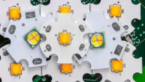
COB technology is also widely used in LED lighting systems. Multiple LED chips can be directly mounted onto a substrate to create a compact and efficient light source.
Advantages include:
- Higher brightness density
- Better heat management
- Compact lighting structure
- Improved optical performance
Industrial Electronics
Industrial control equipment and automation systems often require reliable PCB solutions with high stability. COB packaging helps achieve smaller control modules with improved functionality.
Important Considerations During PCB Proofing
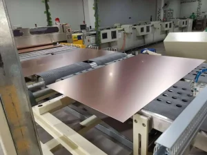
Before moving into mass production, electronic manufacturers usually conduct prototype testing through PCB Proofing.
A well-managed prototype process helps identify design issues, improve manufacturing efficiency, and reduce production risks.
Confirm the Required PCB Quantity
The number of prototype boards should be carefully planned according to testing requirements.
Producing too many samples may increase unnecessary costs, while insufficient quantities may delay verification processes.
Manufacturers should determine the appropriate sample quantity based on:
- Product complexity
- Testing requirements
- Development schedule
- Future production plans
Verify Component Packaging Information
During PCB Assembly, incorrect component packages can cause soldering problems and functional failures.
Before production, engineers should confirm:
- Component package dimensions
- Pin spacing requirements
- Assembly compatibility
- Placement accuracy
Accurate component information ensures smooth assembly and improves prototype reliability.
For professional assembly solutions, explore our PCB Assembly Service.
Perform Complete Electrical Testing
After completing prototype production, comprehensive electrical inspection should be performed.
Testing commonly includes:
- Circuit continuity testing
- Short circuit detection
- Functional verification
- Signal integrity analysis
- Component performance evaluation
A complete testing process ensures the prototype meets design expectations before entering volume manufacturing.
The Role of Professional PCB Manufacturing
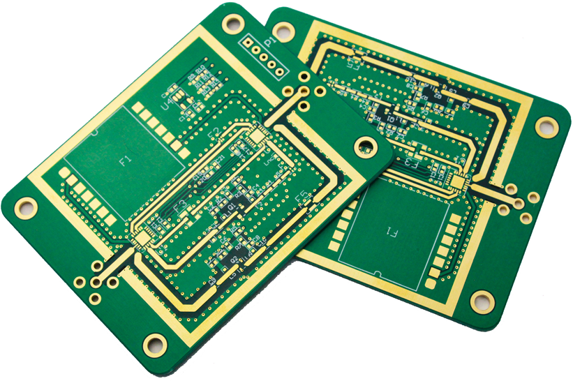
Reliable PCB Manufacturing requires advanced production equipment, strict quality control, and experienced engineering support.
A professional PCB supplier should provide:
- Advanced PCB fabrication technology
- Precise layer alignment
- Reliable material selection
- Automated inspection processes
- Complete production testing
For complex electronic products, cooperation with an experienced PCB manufacturer can significantly improve product quality and shorten development cycles.
Visit our PCB Design Support page to learn how engineering teams optimize PCB designs for production.
How HDI PCB Technology Supports Advanced Electronics
The continuous development of electronic products has increased demand for high-density circuit solutions.
HDI PCB technology enables:
- Smaller via structures
- Higher wiring density
- Better signal performance
- Compact product designs
When combined with advanced packaging technologies like COB, HDI boards provide an effective solution for modern electronic devices requiring high integration.
Applications include:
- Medical equipment
- Automotive electronics
- Communication devices
- Industrial control systems
- Consumer electronics
Conclusion
COB Packaging is an effective chip integration technology that helps electronic manufacturers achieve smaller, lighter, and more efficient products. When combined with HDI PCB technology, it provides excellent support for advanced electronic designs.
Meanwhile, professional PCB Proofing plays a critical role in verifying product performance before mass production. Through reliable PCB Assembly processes and advanced PCB Manufacturing capabilities, companies can improve product reliability, reduce development risks, and accelerate time to market.
Choosing an experienced PCB partner ensures better quality control, efficient production, and long-term manufacturing success.
Explore more solutions through our PCB Assembly Capabilities and start your next electronic project with professional support.