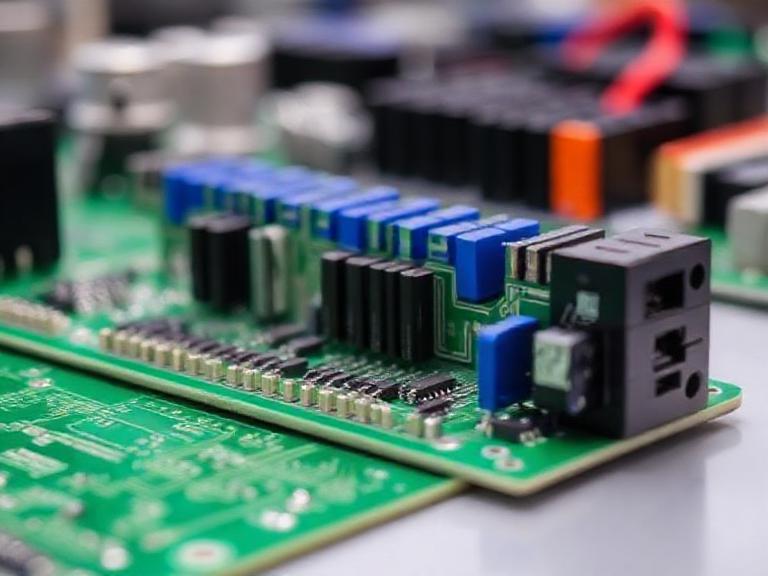
Component Package Types: From DIP to BGA and CSP
Every integrated circuit needs a way to get its tiny internal connections out to the world, and the component package is that interface. It carries the die’s pads out to external terminals, and the terminals connect through the board’s conductors to the rest of the circuit. Along the way the package also mounts, fixes and seals the die, protects it from contamination, and shapes its thermal and electrical behaviour.
That last part is why package choice is a design decision rather than a purchasing convenience. The die is sealed because exposure to airborne contaminants corrodes its circuitry and degrades electrical performance, and the package makes the part easier to handle and ship. Package technology also directly limits how much of the die’s performance can be delivered in circuit and constrains how the board itself can be designed.
What a Package Has to Balance
The quality of a packaging approach is often judged by a single figure: the ratio of die area to package area, where a value closer to one is better because less of the package is doing nothing but carrying the die.
Three further considerations shape the design of a package.
Terminals should be as short as possible, because shorter connections mean less delay. The spacing between terminals, by contrast, should be as generous as possible, so that adjacent conductors do not interfere with each other. And for thermal reasons, a thinner package is better, since a shorter path from die to the outside world removes heat more effectively.
The Two Families and the Direction of Travel
Packages fall into two broad families: the dual in-line through-hole style and the surface mount style. The history runs in a clear direction.
Structurally, the progression went from transistor outlines, to dual in-line, to plastic leaded chip carriers, to quad flat packs, to ball grid arrays, and then to chip scale packages. In materials, it moved from metal and ceramic toward ceramic and plastic, and then largely to plastic — although metal packages remain common in high-reliability work such as military and aerospace applications. In terminal form, it moved from long through-hole leads to short or leadless surface mount terminations, and then to spherical bumps. In assembly, it moved from through-hole insertion to surface mounting, and then to direct attachment.
Through-Hole and Small Outline
DIP — dual in-line package — has terminals emerging from both long sides of the body and is available in plastic and ceramic versions. It is the most widely used through-hole format, covering standard logic, memory and microcomputer circuits.
The small outline family is the surface mount counterpart. The original small outline development dates to the late 1960s, and it spawned a series of derivatives that still fill most of the catalogue: variants with J-formed leads, thin versions, very small versions, shrink versions, thin-shrink versions, small outline transistors and small outline integrated circuits. The family’s proliferation exists because different products needed different compromises between height, terminal count and board area.
Quad Flat Packages
Where terminals are needed on all four sides, quad formats take over.
PLCC is the plastic leaded chip carrier, square with terminals along all four edges. It is much smaller than an equivalent DIP and was designed for surface mounting, with the advantages of a compact outline and high reliability.
TQFP is the thin quad flat package, which uses space efficiently and reduces the board area required, largely because its reduced height and volume suit space-constrained products such as memory cards and network equipment.
PQFP is the plastic quad flat package, used for large and very large scale integration. Its terminals are closely spaced and fine, and the pin count is typically above one hundred.
Thin Small Outline
TSOP — thin small outline package — places terminals around the perimeter of the package body and is well suited to surface mount assembly. Its defining advantage is electrical: the reduced parasitic elements mean that when current changes rapidly, the disturbance to the output voltage is smaller, which suits higher frequency operation. It is also relatively convenient to handle and reasonably reliable. Its main application has been memory.
Array Packages and the Move to Balls
As integration rose and input/output counts climbed, power dissipation grew with them and the demands on packaging became stricter. The BGA — ball grid array — was the response.
Instead of terminals around the perimeter, a BGA places them as an array of round or columnar solder balls underneath the package. The key advantage is geometric: the number of input and output connections can increase substantially without reducing the terminal pitch, which improves assembly yield rather than degrading it. Despite higher power, the package can be soldered by controlled collapse, which improves its thermal and electrical performance. Thickness and weight are lower than earlier formats, parasitic elements are smaller, signal delay is shorter and usable frequency is higher. Because the whole array can be soldered coplanar, reliability is high.
The typical numbers illustrate why the format took over memory. A ball grid array package can increase capacity two to three times within the same volume; at the same capacity, it occupies roughly one third of the volume of a conventional thin small outline part; and it provides a more effective path for heat to escape.
Centre-bonded ball grid variants take the idea further by routing the die’s connections from the centre of the package rather than its perimeter. That layout shortens the signal conduction distance — signal line length can be around a quarter of the perimeter-routed equivalent — which reduces attenuation and improves both noise immunity and electrical performance.
The assembly consequences of array packages are significant, and the process requirements are covered in this look at BGA assembly.
Chip Scale and Direct Attachment
The end point of the progression is the chip scale package, where the package approaches the size of the die itself. A ratio of about 1 to 1.14 between die area and package area is achievable, which means very little area is spent on anything other than the device.
The trade is that the package no longer intervenes between the die and the board to any meaningful degree. Devices mounted this way, including flip chip and wafer-level formats, sit face down on the board and rely on the joints themselves for both electrical connection and mechanical support, so the thermal and mechanical behaviour of the assembly becomes a property of the die, the joints and the board together. That is what makes underfill, careful land pattern design and tight assembly control necessary rather than optional. The practices involved are set out in this review of HDI layout and microvia rules.
Choosing a Package
Temperature and thermal performance. Packages differ in how effectively they remove heat, and a part that is electrically ideal may be thermally unusable in a given enclosure.
Electrical performance. Shorter connections and lower parasitics matter as frequency rises, which is why array and chip scale formats dominate fast interfaces while leaded formats survive at lower speeds.
Pin pitch. Smaller pitch and more terminals increase density and simultaneously raise the demands on assembly, on land pattern design and on inspection.
Assembly capability. A package that the chosen assembly line cannot place, reflow and inspect reliably is not a manufacturing option, whatever its datasheet says.
The practical summary is that packaging is a system decision. The die, the package and the board set each other’s limits, and the smallest available part is not automatically the best one — a point developed further in this discussion of shrinking board area with small components.
FAQ
What does the die-area-to-package-area ratio tell you? How efficiently the package uses its footprint. A ratio close to one means most of the package area is die; a low ratio means much of the package exists to carry and protect a relatively small device.
Why does a BGA tolerate more connections than a leaded package? Because the terminals are distributed across the area underneath rather than crowded around the perimeter. I/O count can grow without the pitch shrinking to an unmanufacturable value.
Are metal and ceramic packages obsolete? No. Plastic dominates consumer and industrial products, but metal and ceramic packages remain in use where the operating conditions or reliability requirements justify them.