SMT PCB Design Principles: Placement and Pads
Design for manufacture sounds like a management concept until it is applied to a specific pad on a specific board. The rules below are the ones that decide whether an assembly runs cleanly through reflow and wave soldering, or comes out with tombstoned passives, bridged leads and joints that were never properly formed. Applying them is most of what SMT PCB design means in practice.
Placement Rules
Orientation is the first consideration. When a board travels along the conveyor of a reflow oven, the long axis of each component should be perpendicular to the direction of travel. A part oriented along the direction of motion is far more likely to drift on its molten solder, or to lift at one end and stand up — the failure known as tombstoning.
Distribution matters as much as orientation. Components should be spread evenly across the board, and high-power devices in particular should be separated rather than clustered. Concentrating heat sources creates local hot regions, and the resulting thermal stress acts directly on the solder joints that fix the components in place.
On assemblies that are populated on both sides, large components should be staggered so that a large part on one side does not sit directly opposite a large part on the other. Two heavy components in the same location add thermal mass precisely where it is least wanted, and the local heat capacity changes how that region reflows.
Wave soldering imposes additional constraints on the side that faces the wave.
Quad-side packages such as PLCC and QFP should not be placed on the wave-soldering side at all. Their leads on all four edges make consistent soldering impractical, and the risk of bridges between adjacent leads is high.
Large surface mount components that are placed on the wave side should have their long axis parallel to the direction of the solder wave, which reduces bridging between adjacent electrodes.
Components of different sizes on the wave side should not be arranged in a single straight line; they should be offset from one another. A large part upstream shadows the smaller parts behind it, and the shadow effect of the wave leaves those joints with insufficient or no solder.
Pad Rules
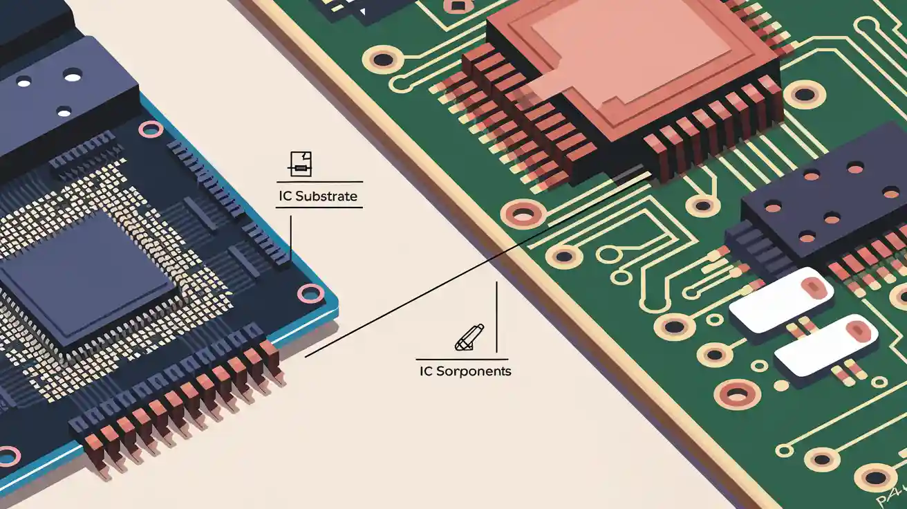
Pads are where the electrical and mechanical requirements meet, and a few rules cover most of the problems.
On the wave-soldering side, the pads of larger components — transistors, sockets and similar — should be enlarged. Extending the pad of a small outline transistor by roughly 0.8 to 1 millimetre is a common measure, and it exists specifically to counteract the shadow effect, which would otherwise leave the joint unsoldered.
Pad size elsewhere should follow the component dimensions. The best results come from a pad whose width equals or slightly exceeds the width of the component’s terminal; a pad narrower than the terminal does not present enough area for a proper fillet, and one that is much wider than necessary wastes routing space and can allow the part to shift.
Where two components must be connected, do not use a single large pad spanning both positions. Solder on a shared pad draws the two parts toward the middle, so they end up out of position. The correct arrangement is separate pads for the two components, joined by a narrower conductor. Where that connection has to carry significant current, several parallel conductors can be used and covered with solder mask, which keeps the current capacity without creating a pool of solder in the wrong place.
Finally, there must be no via in or adjacent to a surface mount pad. During reflow, the solder on the pad melts and wicks down the hole, which produces insufficient joints and open circuits and can continue through to the opposite side of the board, where it forms an unintended connection. Where a via must be used close to a pad, it should be moved clear of the pad boundary or plugged, and the reasons are covered in this discussion of via design rules.
Why These Rules Exist
Each rule above traces back to a physical mechanism rather than to convention. Orientation and staggering address the way heat and molten solder move across a board as it travels through a machine. Pad sizing addresses the surface tension that pulls a component toward the centre of the metal it sits on. The via prohibition addresses capillary action, which is the same force that fills a via under a BGA and can equally empty the paste from a pad above one.
Once the mechanisms are understood, the rules become predictable rather than arbitrary, which matters because no rule list covers every geometry. The general approach to checking a design before it is released, including the checks that catch pad and spacing errors, is described in this discussion of DFM principles for PCBA assembly.
<img src="https://www.gopcba.com/wp-content/uploads/2026/08/773604150_122204755928591289_8347654747047466302_n.jpg" alt="pad design detail for surface mount components” />
Beyond the Pad
Assembly also depends on things that are not on the schematic. Fiducials give the placement machine a reference, and their number and placement are part of the design rather than an afterthought; without them the machine aligns to board edges, and the accuracy of the whole assembly falls. Panelisation, breakaway tabs and the orientation of the array relative to the conveyor belong to the same category, as does the position of the smallest components relative to the process limits of the line that will build the board.
The practical conclusion is that the assembly process belongs in the design conversation from the start. A layout that ignores it can still be manufactured, but it will be manufactured with wider process windows, more inspection, more rework and higher cost — and it will fail on the first design that pushes any parameter.
Solder mask openings are part of the same system, since they determine where paste and solder can actually go, as set out in this note on solder paste mask openings.
Paste Volume Matters as Much as Position
Many defects blamed on placement are actually paste defects. The stencil aperture determines how much paste reaches the pad, and a joint needs both the correct total volume and a balanced volume across a two-terminal component; an imbalance produces the very lift that the orientation rules exist to prevent. Aperture size, stencil thickness and the area ratio between them are therefore part of the same decision as the pad dimensions. Where pads are large but pitches are fine, an aperture deliberately smaller than the pad reduces bridging without leaving the joint short of solder.
FAQ
Why should components be perpendicular to the conveyor direction? Because a component whose long axis aligns with the direction of travel is more likely to drift on molten solder or to lift at one end. Crosswise orientation presents the part to the process in the way that keeps both ends balanced.
Why are vias under pads a problem? Solder wicks into the hole by capillary action during reflow, leaving the joint short of material and, if the hole is open through the board, appearing on the other side as a short circuit.
Why not connect two components with one large pad? Molten solder pulls both components toward the centre of the shared metal, so they move out of position. Separate pads joined by a narrow conductor keep the parts where they were placed.