Compute-in-Memory Chip Test Board PCB: Design and Manufacturing Guide
As compute-in-memory (CIM) technology moves from semiconductor research and development toward commercial production, accurate and reliable chip testing becomes increasingly important. A Compute-in-Memory Chip Test Board PCB serves as the electrical interface between the CIM device and external test equipment, directly affecting signal accuracy, power stability, measurement consistency, and overall test efficiency.
Unlike conventional memory devices, compute-in-memory architectures integrate data storage and computation more closely to reduce data movement and improve processing efficiency. This creates more demanding requirements for the PCB used during chip characterization and validation.
A well-designed Semiconductor Test PCB must support high-speed parallel signals, stable power delivery, high-density interconnections, thermal management, and repeated mechanical operation. PCB material selection, stackup design, impedance control, via technology, surface finish, and inspection processes all contribute to reliable semiconductor testing.
What Is a Compute-in-Memory Chip Test Board PCB?
A Compute-in-Memory Chip Test Board PCB is a specialized circuit board used to connect a compute-in-memory semiconductor device with automated test equipment, power supplies, measurement instruments, and other test interfaces.
Its primary purpose is to provide a controlled electrical environment in which engineers can evaluate the chip’s computing performance, memory behavior, power consumption, latency, bandwidth, and reliability.
During different operating modes, the PCB may need to support:
- Memory read and write testing
- Computing accuracy and performance evaluation
- High-speed data transmission
- Power consumption measurement
- Latency and bandwidth analysis
- Thermal behavior evaluation
- Interface and control signal testing
- Long-duration reliability testing
Because the PCB directly affects the quality of the measured signals, it must be designed as part of the complete semiconductor test system rather than treated simply as an interconnection board.
Core Functions of a Compute-in-Memory Test PCB
1. High-Speed Signal Interconnection
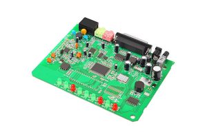
The first major function of a Compute-in-Memory Chip Test Board PCB is to establish a precise electrical connection between the chip and external test equipment.
The PCB must transmit chip output signals to measurement equipment while delivering control commands and test data back to the device. CIM architectures can involve large numbers of parallel data signals, making routing density and signal integrity particularly important.
Poorly controlled traces can introduce:
- Signal reflection
- Crosstalk
- Insertion loss
- Timing skew
- Electromagnetic interference
- Excessive propagation delay
For this reason, controlled impedance routing, carefully designed stackups, matched trace lengths, and optimized return paths are important elements of a high-performance High-Speed PCB.
For projects requiring detailed routing, stackup planning, and manufacturability analysis, professional PCB Design and Layout support can help identify potential signal-integrity and manufacturing issues before fabrication.
2. Stable Power Delivery
Compute-in-memory devices can have significantly different power requirements depending on whether they are operating in memory, computing, or combined compute-and-memory modes.
A test PCB may therefore require multiple power rails to support different functional blocks.
The PCB should provide:
- Dedicated power distribution networks
- Low-impedance power planes
- Proper grounding structures
- Decoupling capacitors
- Power filtering
- Controlled current paths
A poorly designed power distribution network can cause voltage fluctuations and power noise, which may interfere with logic levels and produce inaccurate test results.
Power integrity is therefore closely related to measurement reliability. A stable supply allows engineers to distinguish actual chip behavior from PCB-induced electrical noise.
3. Multi-Scenario Test Support
A CIM test platform may be used to evaluate chips intended for applications such as AI inference, edge computing, high-performance computing, and data-center acceleration.
The test board can therefore incorporate multiple test interfaces and expansion points to support different validation requirements.
Typical parameters include:
- Computing throughput
- Memory bandwidth
- Data transfer efficiency
- Power consumption
- Processing latency
- Thermal performance
- Interface performance
The PCB may also need mechanical interfaces for different heatsinks or thermal modules so that engineers can evaluate chip behavior under different cooling conditions.
Signal Integrity Requirements for Semiconductor Test PCBs
Signal integrity is one of the most important design considerations for a Semiconductor Test PCB.
During high-speed testing, even relatively small discontinuities in PCB routing can affect measurement accuracy. Trace geometry, dielectric properties, via structures, connector transitions, and reference planes all influence signal behavior.
Material Selection
High-speed semiconductor test boards may require materials with suitable dielectric properties, low signal loss, and stable electrical characteristics.
Depending on the signal frequency and application requirements, designers may consider high-Tg or low-loss PCB materials to improve electrical performance.
Material selection should also account for:
- Dielectric constant
- Dissipation factor
- Thermal stability
- Dimensional stability
- Layer thickness
- Copper characteristics
The appropriate material should be selected according to the actual signal frequency, stackup, thermal environment, and testing requirements rather than simply choosing the most advanced material available.
Controlled Impedance
Controlled impedance is essential when high-speed signals must travel between the CIM chip and external test equipment.
The PCB stackup should be established before detailed routing, with trace width, copper thickness, dielectric thickness, and reference-plane configuration considered together.
Differential pairs should maintain appropriate spacing and geometry, while high-speed single-ended signals should also have consistent impedance along the complete signal path.
Via Optimization
Vias introduce parasitic capacitance and inductance into high-speed signal paths. Excessive via transitions can therefore degrade signal quality.
Depending on the board structure, designers may use blind vias, buried vias, or other advanced interconnection technologies to reduce unnecessary signal transitions and support high-density routing.
A suitable PCB Manufacturing process is essential because advanced via structures require tight control over drilling, plating, registration, and layer alignment.
Power Integrity and Grounding Design
Signal integrity alone is not sufficient for a reliable High-Speed PCB. Power integrity must also be carefully controlled.
CIM chips can generate rapid current changes when computing and memory circuits switch simultaneously. If the power distribution network has excessive impedance, these current transients can cause voltage fluctuations.
A robust power distribution structure may include:
- Large-area power planes
- Continuous ground planes
- Short power connections
- Multiple decoupling capacitor locations
- Local high-frequency bypass capacitors
- Optimized return-current paths
Ground-plane continuity is particularly important for high-speed signals. A stable reference plane helps provide a predictable return path and reduces unwanted electromagnetic coupling.
Power and signal routing should therefore be evaluated together during PCB design.
Mechanical and Thermal Stability
A semiconductor test board may be assembled and disassembled many times during the development process. Test sockets, connectors, heatsinks, probes, and fixtures can place repeated mechanical stress on the PCB.
The board should therefore have sufficient structural strength to withstand repeated testing operations.
Depending on the application, designers may consider:
- Increased board thickness
- Reinforced board edges
- Mechanical support structures
- Reinforced connector areas
- Appropriate mounting holes
- High-temperature solder mask
- Reliable surface finishes
Thermal performance is equally important. CIM chips can generate considerable heat during computing-intensive test conditions, and the PCB must remain dimensionally and mechanically stable as the operating temperature changes.
PCB Manufacturing Process Considerations
The manufacturing process directly affects the electrical and mechanical performance of a Compute-in-Memory Chip Test Board PCB.
Pad and Surface Finish
CIM devices may use high-density semiconductor packages with fine-pitch terminals. PCB pad dimensions must therefore be tightly controlled.
The surface finish should provide reliable solderability and resistance to oxidation. Depending on the application, finishes such as ENIG or lead-free HASL may be considered.
For fine-pitch packages, surface flatness and pad consistency are especially important because variations can increase assembly defects and affect electrical connections.
Multilayer Lamination
High-speed semiconductor test boards frequently require multilayer structures to accommodate signal, power, and ground requirements.
Lamination parameters should be carefully controlled to maintain:
- Layer registration
- Dielectric thickness
- Board flatness
- Bonding reliability
- Dimensional stability
Stackup consistency is particularly important when controlled impedance is required.
Precision Drilling and Plating
The reliability of interlayer connections depends on accurate drilling and copper plating.
Critical parameters include:
- Via diameter
- Hole position
- Hole-wall copper thickness
- Registration accuracy
- Plating uniformity
For high-density designs, advanced via structures can help reduce routing constraints while maintaining electrical performance.
PCB Assembly for CIM Test Boards
Fabricating the PCB is only part of the complete test-board development process. Components such as connectors, capacitors, resistors, ICs, sockets, power-management devices, and thermal-control components must also be assembled accurately.
A reliable PCB Assembly process should include engineering review, component verification, SMT or through-hole assembly where required, inspection, and functional testing.
For semiconductor test applications, assembly quality is especially important because solder defects or component-placement errors can be mistaken for chip-level failures.
Important assembly controls include:
- Accurate component placement
- Fine-pitch SMT assembly
- BGA and advanced-package support
- Solder-paste control
- Reflow-profile optimization
- AOI inspection
- X-ray inspection where applicable
- Electrical testing
For early-stage semiconductor development, Prototype PCB Assembly can also shorten the validation cycle by allowing engineers to identify PCB design or assembly problems before committing to larger production quantities.
Testing and Quality Control
Before a Semiconductor Test PCB is delivered, comprehensive inspection should verify both physical construction and electrical performance.
Visual Inspection
Visual inspection should identify issues such as:
- Scratches
- Solder-mask damage
- Pad deformation
- Surface contamination
- Plating defects
- Delamination
- Board-edge damage
Electrical Testing
Electrical testing can verify:
- Continuity
- Isolation
- Short circuits
- Net connectivity
- Resistance
- Controlled impedance where required
For high-speed applications, additional electrical characterization may be required to verify that the board meets the intended transmission requirements.
Environmental Reliability Testing
Depending on the intended test environment, reliability validation may include:
- High-temperature testing
- High-humidity testing
- Thermal cycling
- Mechanical vibration
- Repeated connector or fixture operation
These tests help determine whether PCB performance remains stable during extended semiconductor characterization.
From PCB Prototype to Production
CIM technology is still evolving rapidly, so the PCB design may change frequently during the development process.
A practical development workflow can begin with schematic review and PCB layout, followed by prototype fabrication and assembly. Engineers can then validate signal integrity, power delivery, thermal behavior, and mechanical compatibility.
After design verification, the board can transition into low-volume or larger-scale production.
For projects requiring integrated sourcing and manufacturing support, Components Procurement can simplify the supply chain by coordinating component sourcing with the PCB assembly process.
This approach can reduce the risk of inconsistencies between prototype and production builds and help engineering teams move more efficiently from laboratory validation to commercial deployment.
Why PCB Quality Matters in Compute-in-Memory Development
The performance of a CIM chip cannot be evaluated accurately if the test board introduces significant electrical or mechanical uncertainty.
A high-quality Compute-in-Memory Chip Test Board PCB provides a controlled platform for semiconductor characterization by combining:
- High-speed signal integrity
- Stable power delivery
- Controlled impedance
- High-density interconnection
- Thermal compatibility
- Mechanical durability
- Reliable PCB assembly
- Comprehensive electrical testing
These characteristics help engineers obtain more consistent measurement results and reduce the possibility of PCB-related errors being interpreted as semiconductor defects.
Conclusion
The Compute-in-Memory Chip Test Board PCB is a critical component in the development and validation of next-generation compute-in-memory semiconductors. It connects the device under test with external instrumentation while providing the signal, power, mechanical, and thermal infrastructure required for accurate characterization.
As CIM architectures become more complex, test boards must support higher data rates, denser interconnections, more demanding power requirements, and increasingly sophisticated thermal conditions.
By combining appropriate materials, controlled-impedance routing, optimized power distribution, advanced via structures, reliable PCB Manufacturing, and precision PCB Assembly, engineers can create a stable test platform for semiconductor validation.
A well-engineered Semiconductor Test PCB not only improves testing accuracy but also helps accelerate the transition from chip research and prototyping to reliable production.