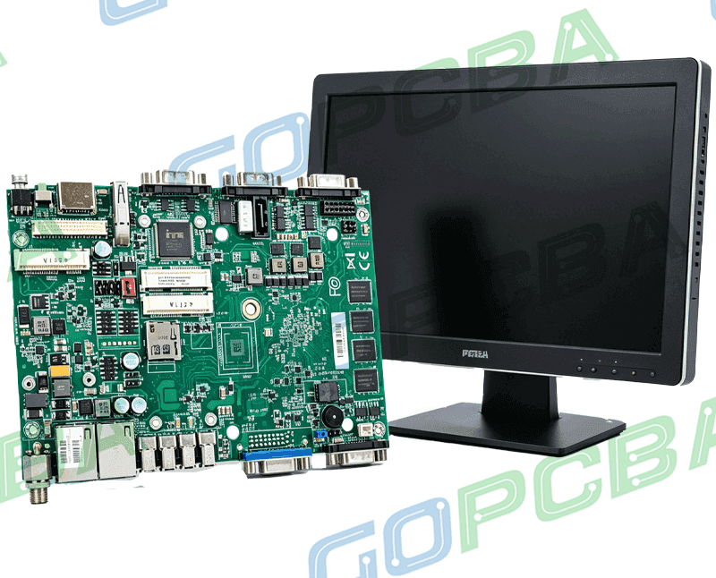
Computer PCB Design: Layer Count and High-Speed Demands
The boards inside computing equipment span an enormous range. A desktop motherboard, a server blade, a solid-state drive controller and a graphics card are all computer PCBs, yet their layer counts, materials and constraints differ completely. What they share is that the interconnect is the limiting factor: the processors are fast enough that the board, rather than the silicon, decides whether the system meets its specification.
This article covers the structure of a computer PCB, the constraints that shape the layer count, and the layout decisions that determine whether high-speed links close.
What Distinguishes a Computer PCB
The defining feature is the number and speed of the parallel interfaces. A server board carries multiple memory channels, several high-speed serial links, a large power delivery network and a management controller. Each of those has its own routing rules, and they compete for the same routing channels.
The second feature is the power delivery requirement. Processor rails run at low voltage and very high current, so the copper and the decoupling network dominate a large part of the board area. On a server board the power delivery network can occupy a third of the layout effort even though it contains no signal routing at all.
Layer Count and Build-Up Structure
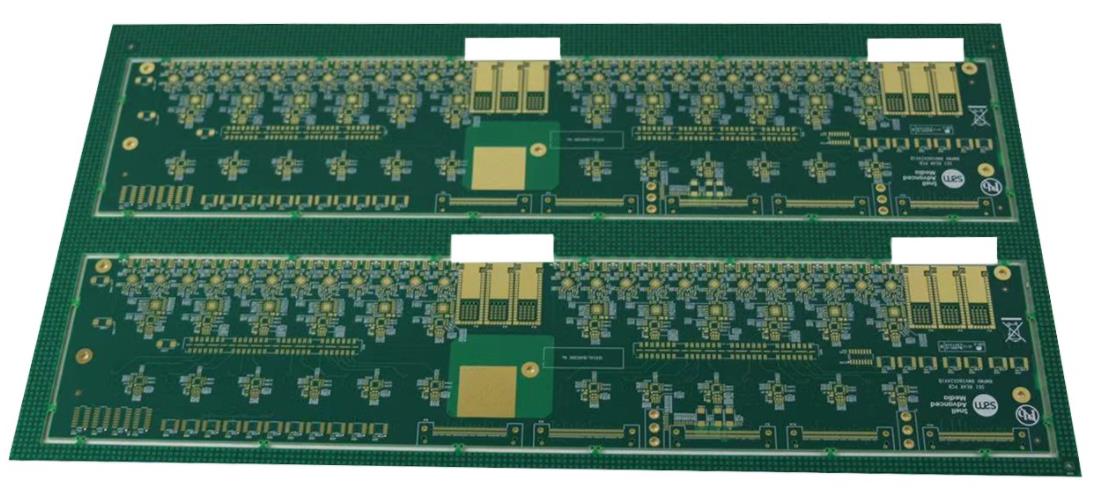
Layer count is driven by the package escape. A processor with a thousand or more balls presents more connections than the outer layers can carry away, so the fanout has to be distributed across several layers, each with vias that do not block the ones below. That is a routing problem that is solved by adding layers rather than by cleverness.
Typical structures run from eight layers for a small controller to sixteen or more for a server board, often with build-up outer layers and buried vias in the core. The stack has to be planned together with the via scheme, because the number of lamination cycles is what sets both the cost and the lead time. The high-speed interface layout rules describe how the escape from a large package interacts with the layer assignment.
High-Speed Signals and Reference Planes
Every high-speed interface needs a continuous reference plane and a controlled impedance. Memory buses are wide and short and must be length matched within a group; serial links are narrow and long and must hold their impedance through connectors and vias. Both are sensitive to the same thing, which is a break in the return path.
The practical rule is that no high-speed net may cross a plane split, and where a change of reference plane is unavoidable, a stitching capacitor has to be placed at the transition. The advantages of a multilayer stack in high-speed designs come almost entirely from the availability of a solid reference plane, which is why a well-planned eight-layer board outperforms a poorly planned twelve-layer one.
Power Delivery and Decoupling
The power delivery network has two parts. The bulk capacitance near the regulator handles the low-frequency load steps, and the high-frequency decoupling spread across the device footprint handles the fast transients. The plane pair between them is the third element, and its low inductance is what allows the whole network to respond quickly.
Copper is the constraint. The current has to travel from the regulator to the device with a resistive drop that is a small fraction of the supply voltage, and the trace width and current calculation gives the geometry. Because the voltage is low, the allowed drop is also small, and the answer is usually several large copper areas on different layers joined by many vias rather than a single wide trace.
Thermal Design
Heat leaves the processor through the package, the socket and the board, and in a computer the board is usually a spreading element rather than the final heatsink. Thermal vias under the device carry heat into the internal planes, which spread it laterally to the areas where it can escape.
The other thermal consideration is that the board itself has to survive the temperature gradients that come with a hot processor and a cold ambient. The coefficient of thermal expansion of the laminate, and the way the copper is balanced across the stack, determine how much the board moves and whether the solder joints on large packages are stressed.
Connectors and Mechanical Interfaces
A computer board is defined by its connectors. The edge connector, the memory slots, the storage connectors and the power inlet are all fixed by mechanical standards, and each one brings a set of layout rules for the escape, the return path and the pin length.
Those rules matter for signal integrity because a connector is a discontinuity. Where a high-speed link passes through a connector, the impedance and the pin assignment determine whether the link closes, and the layout around the connector is as important as the routing in the middle of the board.
Design Process for a Dense Board
Constraint management is the practical answer to the complexity. Each interface is entered as a set of rules covering impedance, spacing, length matching and via structure, and the router is driven by those rules rather than by hand. Where the design has more nets than a person can track, the constraint file becomes the design.
The process should also include a pre-layout review of the stack, the via scheme and the power delivery plan. Finding at that stage that the fanout needs one more layer costs a day; finding it after routing costs a redesign. The mixed-signal layout rules apply wherever analogue or clock circuitry shares the board with the high-speed interfaces.
Materials and Loss at High Data Rates
At the data rates used between a processor and its memory or its storage, the channel loss budget becomes tight enough that the laminate is part of the calculation. Loss rises with frequency, and the dielectric contribution is set by the loss tangent while the conductor contribution is set by the copper surface roughness. Above about ten gigabits per second over a long trace, a low-loss laminate starts to earn its cost.
There is more than one way to buy margin, and the material is not always the cheapest. Shortening the channel, moving it to a layer with a better reference plane, or reducing the number of vias in the path all recover loss without changing the laminate. Those options should be exhausted before the material is changed, because a laminate substitution affects the stack, the impedance targets and the process, and it cannot be reversed late in the project without a full re-qualification.
FAQ
How many layers does a computer PCB need? It depends on the largest package. A small controller may close on eight layers, while a processor with a thousand balls and multiple memory channels typically needs twelve or more, with build-up layers at the surface.
Can a computer board be built on FR-4? In most cases yes. FR-4 is adequate for the interface speeds used in desktop and server equipment over the lengths involved, provided the stack is well designed and the surface roughness is controlled.
Why does decoupling placement matter so much? Because the inductance of the connection between the capacitor and the device limits how quickly the capacitor can respond. A capacitor placed far away is electrically much further away than its physical distance suggests.