Copper Thickness and Current Capacity Planning for PCBs
Two boards can carry the same circuit and behave completely differently under load, because the copper is not the same thickness. Copper thickness determines how much current a trace can carry before it gets too hot, how much voltage it drops along its length, and how much of a thermal path it provides away from a hot component. It is also one of the easiest parameters to specify wrongly, because the number on the drawing is not always the number the finished board contains.
Why Copper Thickness Drives Design
Every conductor has resistance, and that resistance is inversely proportional to the cross-sectional area of the copper. Doubling the thickness halves the resistance for the same trace width, which halves the heat generated for a given current. That single relationship links electrical performance, thermal behaviour and mechanical robustness in one parameter.
The consequence is that copper thickness cannot be chosen at the end of a design. It determines how wide traces must be, how much board area the power distribution consumes, and how much heat can be moved away from a device. Choosing it early and constraining the layout to match is far cheaper than discovering a thermal problem after the first prototype.
Foil Weight, Thickness and Units
Copper is traditionally specified by weight per unit area: one ounce of copper spread over one square foot produces a layer about thirty-five micrometres thick. Half-ounce, one-ounce and two-ounce foils are the common starting points, with heavy copper constructions going to three ounces and beyond for power applications.
The confusion arises because the specified foil weight is the starting point, not the finished result. After plating and etching, the actual thickness on an outer layer can be substantially greater than the foil, while inner layers usually remain close to the laminate foil. When a current capacity calculation is performed, the number that matters is the finished copper thickness, not the foil weight quoted on the fabrication drawing.

Current Capacity and Temperature Rise
Current capacity is not a single number, because it depends entirely on how much temperature rise is acceptable. The standard approach relates the allowable current to the trace cross-section and the permitted temperature rise above ambient, usually ten or twenty degrees Celsius for conservative designs and higher for applications where heat is managed elsewhere.
The relationship is not linear. A trace carrying twice the current does not simply get twice as hot, because the copper resistance rises with temperature and the dissipation depends on the surrounding material. Rules of thumb based on charts are useful for a first pass, but a design that operates near its limit deserves a thermal simulation rather than an estimate. Detailed guidance is available in this overview of high current PCB design.
Trace Width Sizing in Practice
Designers start with the required current, the acceptable temperature rise and the available copper thickness, then solve for the trace width. The result is usually widened further to account for manufacturing tolerance, because a trace that is etched slightly narrow has less copper than the calculation assumed.
Practical constraints then intervene. A trace that is wide enough electrically may not fit, particularly in a dense area or on an inner layer where the available channel is narrow. At that point the options are to use thicker copper, to split the current across multiple layers, or to accept a higher temperature rise with a documented thermal analysis. Making that choice consciously is the difference between a controlled design and an accidental one.
Plating, Etching and Final Thickness
Outer layers receive additional copper during plating, so a one-ounce foil can finish considerably thicker once the plating required for the holes is added. Inner layers receive no such benefit and are typically thinner after lamination because the resin flows and the copper is etched. This asymmetry is why inner layers often carry more current per unit width than designers expect, in the wrong direction.
Etching introduces a second effect. Because the etchant attacks from the side as well as from the top, a trace cross-section is trapezoidal rather than rectangular, with the top narrower than the base. On thick copper the sidewall angle becomes significant and the effective cross-section is smaller than the nominal width multiplied by the thickness. Finer lines on heavy copper are therefore harder to achieve and less predictable, which is why heavy copper designs normally use wider minimum features.
Measuring Copper Thickness
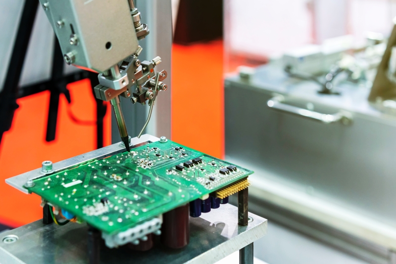
Thickness is verified by several methods, each with its own strengths. Cross sectioning under a microscope gives a direct measurement of a specific trace but is destructive. A four-point probe or an eddy current gauge measures a surface non-destructively but reports an average over a small area. X-ray fluorescence is used for plating thickness and for surface finishes.
Whichever method is used, the measurement location matters. Copper near the board edge etches differently from copper in the centre, and a measurement taken on a test coupon only represents the production board if the coupon experienced the same plating and etching conditions. The principles are shared with other plating thickness checks, and the same discipline of recording where and how the measurement was taken applies.
Inner Layer Versus Outer Layer Behaviour
Inner layers sit between dielectric layers and are therefore thermally insulated on both faces, while outer layers can dissipate heat into the air and into a solder mask. Counter-intuitively, an inner layer trace often runs hotter than an outer layer trace of the same cross-section, because the laminate conducts heat away less effectively than air and radiation combined.
That difference is usually captured by applying a derating factor to inner layer conductors. It is a genuine effect rather than a conservatism, and it shows up clearly in thermal imaging of a loaded board. Where current density is high on multiple inner layers, the layers also heat each other, so the derating should account for the whole stack rather than a single trace. The broader thermal picture is covered in this guide to PCB thermal management.
Power Planes and Thermal Spreading
Power planes behave differently from traces because the current spreads laterally across a wide area. The resistance is low and the temperature rise is modest, but the plane also serves as a heat spreader for components mounted above it. Thicker copper in a plane improves both functions simultaneously.
The limiting factor is usually the connection between the plane and the device, not the plane itself. A thermal relief with narrow spokes can carry far less current than the surrounding plane and can become the hot spot in the design. Where high current and good thermal conduction are both required, direct connection with a controlled soldermask opening is often better than a traditional relief.
Specifications and Tolerances
A fabrication drawing should state the finished copper thickness for each layer, the acceptable tolerance and the measurement method. Quoting only the foil weight leaves the finished thickness undefined and creates disputes later. For heavy copper, the tolerance band is wider and the minimum trace width and spacing must be stated explicitly, because the etching behaviour changes.
Tolerance compounds with temperature rise. A trace at the thin end of the tolerance band and operating at the higher end of the ambient range will be noticeably hotter than the nominal calculation suggests. Designing to the worst case, rather than to the nominal, is the only way to guarantee that the finished product behaves as predicted.
FAQ
What does one ounce of copper mean? It means one ounce of copper per square foot of area, which corresponds to a thickness of roughly thirty-five micrometres or about 1.4 thousandths of an inch. The unit is a legacy of the foil rolling industry, and it describes the starting foil rather than the finished thickness on the board.
Can I simply widen a trace instead of using thicker copper? Often you can, but widening consumes routing area and may not fit on a dense board. Thicker copper keeps the width manageable but changes etching behaviour, minimum feature sizes and cost. The right answer depends on which resource is scarce in that particular design.
Why do inner layers need a derating factor? Because an inner layer trace is surrounded by laminate on both sides, which conducts heat away less effectively than the air and radiation available to an outer layer. As a result, an inner layer trace of the same cross-section runs hotter, and the design must allow for it rather than treating all layers as equivalent.