Custom PCB Assembly: Process, Design Considerations, Technologies, Benefits, and Applications
Printed circuit boards (PCBs) provide the essential platform for electrically and mechanically interconnecting electronic components, enabling products to achieve their intended functionality, performance, and reliability. While conventional PCB manufacturing and assembly processes are designed to meet predefined specifications and production requirements, many modern products demand much greater flexibility.
As industries continue to develop increasingly compact, intelligent, connected, and application-specific products, the demand for custom PCB assembly has grown significantly. From prototype development and low-volume production to specialized industrial equipment and advanced IoT devices, customized PCB solutions allow engineers to optimize board architecture, component selection, manufacturing processes, testing methods, and overall product performance.
Although standard PCB manufacturing follows established quality management systems to ensure consistent production, customized projects often require additional engineering analysis, process validation, material verification, and quality controls. This article explains what custom PCB assembly is, why it is important, how the process works, key design considerations, technologies used, major benefits, applications, and how to select the right manufacturing partner.
What Is Custom PCB Assembly?
Custom PCB assembly is the process of manufacturing and assembling a printed circuit board according to the specific electrical, mechanical, environmental, and functional requirements of a particular product or project.
Unlike standardized PCB solutions, custom electronic assembly provides greater flexibility in areas such as circuit architecture, board dimensions, layer count, material selection, component selection, assembly technology, and testing requirements.
A custom PCB can be optimized for factors including:
- Circuit complexity and routing density
- PCB dimensions and mechanical constraints
- Number of layers
- Copper thickness
- PCB substrate and dielectric materials
- Component availability and lifecycle
- Surface finish
- Thermal management
- Signal integrity and impedance control
- Electromagnetic compatibility (EMC)
- Assembly technology
- Testing and inspection requirements
This flexibility enables designers and manufacturers to optimize the complete electronic assembly rather than simply adapting a standard PCB to a new application.
Why Is Custom PCB Assembly Important?
Engineers develop custom PCBs when standard products cannot adequately satisfy the technical or operational requirements of a specific application.
Standard components and standard PCB assemblies generally have predefined dimensions, electrical characteristics, interfaces, manufacturing processes, and performance parameters. These standardized solutions are highly effective for large-scale production, but they may not provide sufficient flexibility for specialized products.
Custom PCB assembly allows multiple functions and components to be integrated into a single optimized system. For example, a custom board may combine power management, processing, communication interfaces, sensors, memory, connectors, and control circuitry within a compact assembly.
Customization can therefore help manufacturers:
- Reduce product size
- Improve electrical performance
- Optimize thermal behavior
- Increase functional integration
- Improve reliability
- Support specialized interfaces
- Simplify system architecture
- Enable future product upgrades
For technically demanding products, customization can become an important part of the overall product-development strategy.
Custom PCB Assembly Process
The PCB assembly process for customized products generally requires more engineering coordination than a standard production program. Each stage must be adapted to the project’s electrical, mechanical, manufacturing, and quality requirements.
1. Component Selection and Verification
Component selection is one of the most important stages of a custom PCB project.
A customized assembly may contain components sourced from multiple manufacturers and suppliers. Each component must therefore be evaluated for electrical specifications, package type, operating temperature, availability, lifecycle status, and long-term supply stability.
Particular attention should be given to:
- New or recently introduced components
- End-of-life (EOL) components
- Obsolete components
- Custom mechanical components
- Fine-pitch components
- High-reliability components
- Components with long procurement lead times
Before finalizing the bill of materials (BOM), manufacturers should verify component specifications, approved manufacturer lists (AML), availability, and potential alternatives.
For custom components, prototype validation should be completed before mass production whenever possible.
2. PCB Manufacturing
The custom PCB assembly process begins with manufacturing the bare PCB.
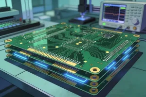
Depending on the design, the manufacturing process may include material preparation, inner-layer imaging, etching, lamination, drilling, copper plating, outer-layer processing, solder mask application, silkscreen printing, surface finishing, and final inspection.
For multilayer PCBs, accurate layer alignment and lamination control are particularly important.
Advanced designs may also require:
- Microvias
- Blind and buried vias
- HDI structures
- Controlled impedance
- Fine-pitch pads
- Heavy copper
- Flexible or rigid-flex structures
- Specialized dielectric materials
Drilling and via fabrication must be carefully controlled because dimensional deviations can affect electrical connectivity and reliability.
The solder mask protects copper features from oxidation and accidental solder bridging, while silkscreen markings provide important reference information for component placement, inspection, repair, and troubleshooting.
Depending on the project architecture, multiple PCBs may also need to be manufactured as separate subassemblies and later integrated into a larger electronic system.
3. PCB Assembly
After the bare PCB has passed inspection, components are mounted using the appropriate assembly technology.
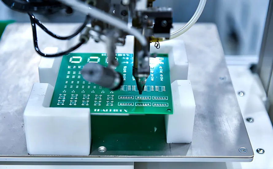
For surface-mount technology (SMT), solder paste is first deposited onto the designated pads using a stencil printing process. A pick-and-place machine then accurately positions surface-mount devices (SMDs) according to the programmed placement data.
The assembled board subsequently enters a reflow soldering oven. The solder paste is heated according to a controlled thermal profile, allowing the solder alloy to melt and form reliable solder joints between the components and PCB pads.
Through-hole technology (THT) components may be inserted manually or automatically depending on the design and production volume. Wave soldering, selective soldering, or manual soldering can then be used according to the component and assembly requirements.
During assembly, manufacturers must carefully control:
- Component orientation
- Polarity
- Placement accuracy
- Solder paste volume
- Reflow profile
- Solder joint quality
- Component height
- Clearance between components
- Connector alignment
Connectors, cables, mechanical parts, heat sinks, and other secondary components can then be integrated to complete the customized electronic assembly.
4. Inspection, Testing, and Troubleshooting
Testing and validation are essential for ensuring the reliability of a custom PCB assembly.
Visual inspection is normally performed throughout the production process. Depending on project requirements, automated optical inspection (AOI) can identify component placement errors, solder bridges, insufficient solder, missing components, polarity issues, and other visible defects.
Additional testing may include:
- In-circuit testing (ICT)
- Flying probe testing
- Functional testing (FCT)
- Boundary-scan testing
- Insulation and dielectric withstand testing
- Programming and firmware verification
- Environmental testing
- Thermal testing
- Vibration testing
- EMC/EMI testing
For products intended to operate in harsh environments, additional reliability and compliance testing may be necessary.
A well-designed test strategy should identify defects as early as possible, reduce rework, and provide traceable production data for continuous quality improvement.
Key Design Considerations for Custom PCB Assembly
A well-designed and thoroughly documented PCB assembly is easier to manufacture, inspect, test, and maintain. Design teams should therefore consider manufacturability, assembly, testing, sourcing, and future maintenance during the initial design stage.
Layout Optimization and Component Placement
PCB layout optimization is critical to improving manufacturing efficiency and electrical performance.
Designers should organize components according to their functional relationships while maintaining appropriate electrical and mechanical clearance.
Important considerations include:
- Short and efficient signal paths
- Proper power and ground distribution
- Controlled impedance where required
- Thermal management
- Adequate component spacing
- Reduced electromagnetic interference
- Efficient routing
- Accessible test points
- Appropriate connector placement
High-speed and RF designs require additional attention to signal integrity, return paths, grounding, transmission-line geometry, and impedance control.
Thermal components such as power ICs, MOSFETs, regulators, and processors should be positioned and designed with adequate thermal dissipation in mind.
Design for Manufacturability and Assembly
Design for Manufacturing (DFM) and Design for Assembly (DFA) should be incorporated into custom PCB projects as early as possible.
A design that is electrically functional may still be difficult or expensive to manufacture if it contains unnecessary complexity, insufficient spacing, difficult-to-source components, or problematic assembly structures.
DFM and DFA reviews can help identify:
- Insufficient pad spacing
- Incorrect footprints
- Difficult component orientations
- Excessive component density
- Inadequate solder mask clearance
- Difficult-to-access test points
- Unnecessary assembly operations
- Components with high supply-chain risk
Early design reviews can significantly reduce manufacturing problems and engineering changes later in the project.
Standardization and Validation of New Components
Custom projects frequently require components that have not previously been used in the manufacturer’s standard production portfolio.
These components should be carefully evaluated and validated before volume production.
A structured qualification process can include:
- Datasheet verification
- Manufacturer qualification
- Package and footprint verification
- Prototype assembly
- Electrical testing
- Thermal and environmental validation
- Reliability assessment
- Production approval
Any uncontrolled component change can affect PCB performance, assembly quality, and product reliability. Maintaining strict BOM and revision control is therefore essential.
Early Collaboration with the Assembly Partner
Early communication with the PCB assembly partner can significantly improve project efficiency.
Rather than waiting until the design is complete, engineering teams can work with the manufacturer during the design stage to evaluate:
- PCB manufacturability
- Component availability
- Assembly feasibility
- Stencil design
- Reflow requirements
- Testing strategy
- Production volume
- Cost optimization
- Potential design risks
Experienced manufacturers can often identify problems before prototypes are produced, reducing unnecessary engineering iterations and development costs.
Establishing an Appropriate Test Strategy
Standard testing methods may not be sufficient for highly customized products.
The test strategy should be developed according to the product’s intended application and risk profile. The manufacturer and customer should jointly define inspection criteria, electrical test requirements, functional specifications, acceptance standards, and traceability requirements.
For complex products, testing may include both production-line testing and independent third-party certification.
Technologies Used in Custom PCB Assembly
As electronics continue to become smaller, faster, and more integrated, PCB manufacturers are adopting advanced technologies to support increasingly complex customized projects.
Smart Manufacturing and Automation
Modern PCB assembly facilities increasingly integrate automation, manufacturing execution systems (MES), real-time production monitoring, and intelligent quality-control technologies.
Common technologies include:
- Automated SMT placement
- Automated solder paste inspection (SPI)
- Automated optical inspection (AOI)
- Automated component verification
- Real-time production monitoring
- Equipment condition monitoring
- Digital inventory management
- Manufacturing traceability
These technologies improve process consistency while reducing human error and increasing production efficiency.
Component Miniaturization
Electronic products continue to demand smaller dimensions and greater functionality.
Fine-pitch packages, micro-BGA components, CSP packages, and other compact components enable manufacturers to achieve higher circuit density.
However, component miniaturization also increases the requirements for:
- Placement accuracy
- Stencil printing
- Solder paste control
- Reflow profiling
- Inspection resolution
- PCB fabrication accuracy
Advanced manufacturing technologies are therefore essential for reliable high-density assemblies.
Flexible and Rigid-Flex PCBs
Flexible PCBs and rigid-flex PCBs are increasingly used in applications where conventional rigid boards cannot provide sufficient mechanical flexibility or space efficiency.
Their advantages include:
- Reduced weight
- Improved space utilization
- Reduced wiring complexity
- Resistance to repeated bending
- Improved integration in compact products
- Greater freedom in mechanical design
Flexible and rigid-flex technologies are particularly valuable for compact electronic devices, wearable equipment, medical products, automotive electronics, and other applications with complex mechanical constraints.
Advanced Quality Control
Higher production speeds require equally advanced quality-control systems.
Modern manufacturing environments can combine automated inspection, real-time process monitoring, statistical process control (SPC), traceability systems, and data analysis to improve product consistency.
Artificial intelligence and machine-learning technologies can further assist with defect classification, inspection optimization, anomaly detection, and predictive maintenance.
These capabilities can help manufacturers detect defects earlier, improve traceability, reduce inspection costs, and identify potential process problems before they result in large-scale production losses.
Benefits of Custom PCB Assembly
The growing adoption of customized electronics has made custom PCB assembly increasingly important across many industries.
Multiple Functions in a Single Assembly
A customized PCB can integrate multiple functions into one compact electronic assembly.
For example, a single board may combine:
- Power management
- Processing units
- Memory
- Sensors
- Communication interfaces
- Input/output interfaces
- Control circuits
- Connectors
This high level of integration can reduce the number of separate modules and simplify the overall system architecture.
Improved Performance
Custom PCB design allows engineers to optimize electrical and mechanical characteristics for a specific application.
Designers can adjust circuit architecture, component selection, signal routing, thermal management, power distribution, and communication interfaces according to the required performance targets.
This makes it possible to overcome limitations associated with generic or standardized PCB solutions.
Greater Upgrade Potential
Custom PCB assemblies can be designed with future upgrades in mind.
Engineers may reserve interfaces, processing capacity, memory, or expansion connections to accommodate future product revisions.
This approach can extend product lifecycles and reduce the need for complete hardware redesigns when new functions are introduced.
Better Space and Cost Optimization
Although the initial engineering cost of a custom PCB may be higher, optimized integration can reduce the number of individual modules, cables, connectors, and mechanical components required in the final system.
For medium- and high-volume applications, this integration can potentially reduce total system cost and assembly complexity.
Applications of Custom PCB Assembly
Custom PCB assembly supports a wide range of industries because it allows electronic systems to be optimized around specific functional and mechanical requirements.
IoT Solutions
Internet of Things (IoT) products often require compact designs that combine sensors, processors, wireless communication, power management, and data interfaces.
Custom PCBs allow these functions to be integrated into a single compact platform while supporting application-specific connectivity and power requirements.
Industrial Automation Systems
Industrial automation is another major application area.
Industrial control systems often require customized combinations of processors, sensors, communication interfaces, power circuits, relays, connectors, and control modules.
Custom PCB assemblies can therefore be designed around specific machines, production lines, controllers, monitoring systems, and automation equipment.
Customized Consumer Electronics
Consumer products increasingly require application-specific functions and compact mechanical designs.
Custom PCBs allow manufacturers to integrate user-specific functions while optimizing product size, interfaces, power consumption, and overall performance.
Research and Development Projects
Research institutions, engineering teams, and technology developers frequently require custom electronics for experimental platforms, prototypes, evaluation equipment, and proof-of-concept systems.
Custom PCB assembly enables engineers to rapidly implement specialized circuits and modify designs as development requirements evolve.
Automotive and Transportation Electronics
Automotive electronics require high reliability, thermal stability, vibration resistance, and long-term component availability.
Custom PCB assemblies can be designed for vehicle control systems, sensors, communication modules, power electronics, infotainment systems, and other specialized automotive applications.
Medical and Industrial Equipment
Medical and industrial equipment frequently requires specialized interfaces, compact electronic architectures, and strict testing requirements.
Custom PCB assembly provides the flexibility needed to integrate application-specific control, sensing, communication, and monitoring functions.
Custom PCB Assembly vs. Standard PCB Assembly
The main difference between custom and standard PCB assembly lies in the degree of design and manufacturing flexibility.
Custom PCB assembly is optimized around a specific product or project, while standard PCB assembly focuses on repeatable production using predefined designs, components, and processes.
| Feature | Custom PCB Assembly | Standard PCB Assembly |
|---|---|---|
| Purpose | Designed for specific project requirements | Designed for standardized products |
| Design Approach | Highly flexible PCB layout, materials, and components | Uses predefined PCB specifications and components |
| Customization | High degree of customization | Limited customization |
| Initial Cost | Usually higher due to engineering and validation | Generally lower for established designs |
| Lead Time | May be longer due to development and validation | Usually shorter for mature products |
| Technical Support | Requires extensive engineering communication | Usually requires less engineering support |
| Testing | Application-specific testing may be required | Standardized testing procedures |
| Typical Applications | Prototypes, specialized equipment, low-volume and complex products | Established products and high-volume production |
| Upgrade Potential | High | Usually limited |
Neither approach is universally better. The appropriate solution depends on product complexity, production volume, development stage, performance requirements, and cost targets.
How to Choose a Custom PCB Assembly Manufacturer
Selecting the right custom PCB assembly manufacturer is an important decision because the supplier’s engineering capabilities, manufacturing capacity, quality system, and supply-chain management can directly affect product performance and project schedules.
Technical Expertise and Manufacturing Capabilities
A qualified PCB manufacturer should have experience with different PCB structures, assembly technologies, component packages, and testing requirements.
When evaluating a supplier, consider whether it can support:
- SMT and through-hole assembly
- Multilayer PCBs
- HDI PCBs
- Flexible and rigid-flex PCBs
- Fine-pitch components
- Prototype and low-volume production
- High-volume manufacturing
- Advanced inspection and testing
The manufacturer should also be capable of reviewing customer designs and providing practical engineering recommendations.
Production Capacity and Quality Assurance
Production capacity is only one part of supplier selection. A reliable manufacturer should also demonstrate effective process control and quality management.
Important indicators include:
- Quality management systems
- Manufacturing certifications
- Process control procedures
- Automated inspection equipment
- Traceability systems
- Supplier management
- Production capacity
- Equipment maintenance
- Continuous improvement programs
These factors help ensure that customized products can be manufactured consistently and delivered according to schedule.
Engineering Support
Engineering support is particularly important for customized projects.
A strong manufacturing partner should participate in design reviews rather than simply manufacture the files provided by the customer.
Useful engineering services may include:
- DFM analysis
- DFA analysis
- BOM review
- Component lifecycle analysis
- PCB layout review
- Prototype support
- Assembly process optimization
- Test strategy development
- Failure analysis
Effective communication between the customer and manufacturer can significantly reduce development risks.
Cost and Quality Balance
Cost is an important consideration, but selecting a PCB manufacturer solely according to the lowest quotation can create long-term risks.
Low-cost components or insufficient process controls may reduce the initial project cost while increasing the risk of field failures, rework, warranty claims, and supply-chain problems.
A better approach is to evaluate total cost of ownership, including:
- Component quality
- Manufacturing cost
- Engineering cost
- Testing cost
- Yield
- Lead time
- Reliability
- Long-term component availability
The best supplier is not necessarily the cheapest supplier, but the one that provides an appropriate balance between cost, quality, reliability, engineering capability, and delivery performance.
Why Choose Kingda for Custom PCB Assembly?
Kingda provides customized PCB manufacturing and assembly solutions for customers with different technical and production requirements.
From prototype development and engineering validation to small-batch production and larger-scale manufacturing, Kingda can support customers throughout the PCB development and assembly lifecycle.
A professional custom PCB assembly partner should be able to:
- Analyze project requirements
- Review PCB and BOM data
- Identify potential manufacturing risks
- Optimize assembly processes
- Support prototype development
- Implement inspection and testing procedures
- Provide production traceability
- Maintain consistent quality control
- Support product improvements and future revisions
For complex PCB projects, close cooperation between the customer and manufacturer can help shorten development cycles, improve first-pass yield, reduce manufacturing risks, and create a more reliable final product.
Conclusion
Custom PCB assembly gives product designers and engineers greater freedom to develop electronic systems around specific functional, mechanical, electrical, and environmental requirements.
Compared with standardized PCB solutions, customized assemblies can provide greater flexibility in component selection, circuit architecture, board dimensions, manufacturing technology, testing, and future upgrades.
As electronics continue to become smaller, smarter, faster, and more integrated, technologies such as HDI, fine-pitch assembly, flexible PCBs, rigid-flex PCBs, automated inspection, intelligent manufacturing, and AI-assisted quality control will continue to expand the capabilities of custom PCB manufacturing.
For businesses developing specialized electronics, selecting an experienced manufacturing partner is equally important. A capable supplier should provide not only production capacity but also engineering support, DFM/DFA expertise, component sourcing, quality assurance, testing, traceability, and long-term technical support.
With comprehensive engineering and manufacturing capabilities, Kingda can help customers transform customized PCB concepts into reliable and production-ready electronic assemblies.