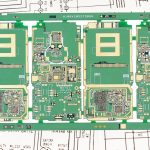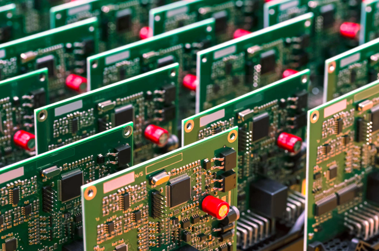
Custom PCB Assembly refers to manufacturing and assembling printed circuit boards according to the specific electrical, mechanical, thermal, environmental, and production requirements of a product.
Unlike standardized circuit boards designed for general applications, a Custom PCB is developed around the requirements of a particular electronic system. Customization can involve the PCB layer structure, materials, dimensions, component selection, circuit layout, surface finish, assembly technology, testing requirements, and mechanical integration.
A successful custom PCB project requires close coordination between PCB Design and manufacturing. Design decisions made during the development stage can directly affect fabrication difficulty, assembly efficiency, testing, reliability, and total production cost.
Custom PCB solutions are widely used in industries such as automotive electronics, medical equipment, industrial automation, telecommunications, consumer electronics, aerospace, energy systems, and specialized electronic equipment.
Why Use Custom PCB Assembly?
Standard PCB solutions may not always satisfy the requirements of a specialized electronic product. A custom manufacturing approach allows the PCB and assembly process to be optimized for the actual application.
Key benefits include:
- Application-specific design
- Flexible component selection
- Optimized PCB dimensions
- Improved electrical performance
- Better thermal management
- Higher component density
- Greater mechanical integration
- Optimized manufacturing cost
- Support for specialized testing
- Improved product scalability
The objective is not simply to create a unique circuit board, but to develop a PCB assembly that provides the required performance while remaining practical to manufacture.
Different Types of Custom PCBs
Before starting a Custom PCB Assembly project, it is important to determine the appropriate PCB structure.
Single-Sided PCB
A single-sided PCB contains conductive circuitry on one side of the substrate.
It has a relatively simple structure and is commonly used in cost-sensitive electronic products with lower circuit density.
Double-Sided PCB
A double-sided PCB contains conductive layers on both sides of the substrate.
Vias can be used to establish electrical connections between the two sides, allowing greater routing flexibility and component density than a single-sided board.
Multilayer PCB
A multilayer PCB contains multiple conductive layers separated by dielectric materials.
Multilayer construction provides greater routing capacity and is commonly used for complex electronic systems requiring high circuit density, power distribution, controlled impedance, or improved signal integrity.
Rigid PCB
Rigid PCBs use a non-flexible substrate and represent one of the most common PCB structures.
FR-4 is widely used for general-purpose rigid PCB applications, while specialized laminates may be selected for high-frequency, high-temperature, or other demanding applications.
Flexible PCB
Flexible PCBs use flexible substrates that allow the circuit to bend or conform to a specific mechanical structure.
They are useful where space is limited or where the PCB needs to accommodate movement, folding, or complex three-dimensional packaging.
Rigid-Flex PCB
Rigid-flex PCBs combine rigid and flexible sections into a single integrated circuit structure.
This approach can reduce the number of connectors and interconnections while allowing the PCB to fit complex mechanical assemblies.
Benefits of Custom PCB Design
Design and Functional Flexibility
One of the main advantages of a Custom PCB is the ability to optimize the circuit for a specific application.
Engineers can select:
- PCB dimensions
- Number of layers
- Copper thickness
- Dielectric materials
- Component packages
- Connector positions
- Routing structures
- Thermal solutions
- Surface finishes
- Test points
This flexibility allows the PCB to be designed around the product instead of forcing the product to conform to a standard board.
Cost Optimization
Customization does not necessarily mean higher production costs.
A properly optimized design can eliminate unnecessary components, reduce board size, improve panel utilization, simplify assembly, and select materials according to actual performance requirements.
Cost should therefore be evaluated across the complete product lifecycle rather than only by comparing the initial PCB quotation.
Improved Efficiency
A well-designed custom board can integrate functions that might otherwise require multiple PCBs, cables, or connectors.
Reducing unnecessary interconnections can simplify assembly and potentially improve system reliability.
Improved Electrical Performance
Custom PCB Design allows engineers to optimize component placement and signal routing according to system requirements.
Important considerations include:
- Signal integrity
- Power integrity
- Impedance control
- Grounding
- Return paths
- Crosstalk
- EMI and EMC
- High-speed signal routing
These considerations are especially important for high-speed digital, RF, automotive, and communication applications.
Better Thermal Management
Power electronics and high-performance components can generate significant heat.
A custom PCB can incorporate appropriate thermal strategies, such as:
- Larger copper areas
- Thermal vias
- Heavy copper
- Metal-core structures
- Heat-spreading layers
- Appropriate component placement
The thermal design should be evaluated together with the enclosure and system-level cooling strategy.
Custom PCB Assembly Process
A typical Custom PCB Assembly workflow includes design review, PCB fabrication, component preparation, SMT assembly, through-hole assembly when required, soldering, inspection, and testing.
1. Schematic and PCB Layout
The process begins with the electrical schematic and PCB layout.
Design files may include:
- Schematic files
- PCB layout files
- Gerber files
- Drill files
- BOM
- Pick-and-place files
- Assembly drawings
- Fabrication specifications
- Testing requirements
The design should be reviewed to ensure that the manufacturing data is complete and consistent.
2. DFM Review
A Design for Manufacturing (DFM) review is an important part of custom PCB development.
DFM analysis can identify potential problems before production begins, including:
- Insufficient component clearance
- Inappropriate pad dimensions
- Difficult-to-manufacture traces
- Improper via structures
- Component placement problems
- Insufficient test-point access
- Panelization limitations
- Assembly-side clearance issues
Early DFM analysis can reduce manufacturing iterations and improve the transition from prototype to production.
3. PCB Fabrication
After the design is finalized, the bare PCB is manufactured according to the approved specifications.
Depending on the board structure, fabrication may include:
- Material preparation
- Inner-layer imaging
- Lamination
- Drilling
- Plating
- Outer-layer imaging
- Etching
- Solder mask application
- Surface finishing
- Electrical testing
- Final inspection
The actual process varies according to PCB structure, materials, layer count, and manufacturing technology.
4. Solder Paste Printing
For SMT production, solder paste is deposited onto the PCB pads through a stencil.
Printing quality directly affects solder-joint formation.
Important parameters include:
- Stencil thickness
- Aperture design
- Solder paste properties
- Printing speed
- Squeegee pressure
- Separation speed
- PCB support
SPI can be used to measure solder paste deposition and identify printing problems before component placement.
5. Component Placement
After solder paste printing, automated pick-and-place equipment positions SMT components on the PCB.
The placement process must account for:
- Component orientation
- Package type
- Polarity
- Placement accuracy
- Feeder configuration
- Component spacing
- Board support
Proper placement programming is particularly important for custom boards containing fine-pitch ICs, BGA packages, connectors, or mixed component technologies.
6. Reflow Soldering
The populated PCB passes through a reflow oven to form solder joints between the components and PCB pads.
The reflow profile should be developed according to the solder paste, PCB materials, component specifications, and assembly requirements.
A typical reflow process includes:
Preheating → Thermal Soak → Reflow → Cooling
The actual temperature profile should be verified through appropriate thermal profiling rather than relying on a generic temperature setting.
7. Through-Hole Assembly
If the design includes through-hole components, they can be installed after or alongside SMT assembly depending on the manufacturing process.
Possible soldering methods include:
- Wave soldering
- Selective soldering
- Manual soldering
The appropriate method depends on the component type, PCB design, production volume, and assembly requirements.
8. AOI Inspection
Automated Optical Inspection (AOI) uses cameras and image-processing algorithms to identify many visible assembly defects.
AOI can detect issues such as:
- Missing components
- Incorrect component placement
- Polarity errors
- Component misalignment
- Solder bridging
- Abnormal solder joints
AOI provides efficient inspection for many SMT assemblies, but it should be combined with other inspection and testing methods when required.
9. X-Ray Inspection
X-ray inspection is useful when solder joints cannot be visually inspected.
Typical applications include:
- BGA packages
- QFN packages
- Bottom-terminated components
- Other hidden solder connections
Whether X-ray inspection is necessary depends on the product’s package types, reliability requirements, and quality-control plan.
10. Electrical and Functional Testing
PCB Testing verifies whether the completed assembly meets the required electrical and functional specifications.
Testing may include:
- Continuity testing
- Insulation testing
- Flying-probe testing
- ICT
- Programming
- Functional testing
- System-level testing
Test requirements should ideally be defined during the design stage so that appropriate test points and access can be incorporated into the PCB.
Quality Considerations for Custom PCB Assembly
Because custom products may have unique requirements, quality control should be established according to the actual application.
A comprehensive quality plan may include:
- Incoming material inspection
- PCB fabrication inspection
- Component verification
- Solder paste inspection
- Placement verification
- Reflow profile verification
- AOI
- X-ray inspection when required
- Electrical testing
- Functional testing
- Final inspection
For demanding applications, additional environmental, thermal, mechanical, or reliability testing may be appropriate.
Factors Affecting Custom PCB Assembly Cost
The cost of PCB Manufacturing and assembly depends on the specific requirements of the project.
Important cost factors include:
PCB Structure
Layer count, board thickness, copper weight, via technology, and surface finish can all affect fabrication costs.
Material Selection
Standard FR-4 may be suitable for many applications, while high-Tg, high-frequency, flexible, ceramic, metal-core, or other specialized materials can increase material and processing costs.
Board Size
Larger boards generally consume more material and may affect panel utilization.
Component Count
A greater number of components generally increases placement, soldering, inspection, and testing requirements.
Component Package
Fine-pitch, BGA, QFN, and other specialized packages may require tighter manufacturing controls and additional inspection.
Production Quantity
Prototype and low-volume orders generally have higher unit costs because setup, engineering, tooling, and other fixed costs are distributed across fewer boards.
Testing Requirements
Additional electrical, functional, environmental, or reliability testing can increase manufacturing time and cost.
How DFM Helps Optimize Custom PCB Assembly
DFM should be considered from the beginning of the development process.
Effective DFM can help identify opportunities to:
- Simplify PCB structures
- Improve component accessibility
- Reduce unnecessary manufacturing steps
- Optimize panel utilization
- Improve automated assembly
- Reduce potential soldering defects
- Improve test accessibility
- Reduce rework
For a new product, DFM should ideally be performed before prototype production rather than after manufacturing problems have already occurred.
Choosing a Custom PCB Assembly Supplier
Selecting a suitable supplier is an important part of a successful custom PCB project.
Price and Total Cost
Compare the complete manufacturing cost rather than focusing only on the PCB or assembly unit price.
The quotation should clearly identify major cost components where appropriate.
Lead Time
Actual lead time depends on PCB complexity, material availability, component sourcing, assembly requirements, testing, and production capacity.
A supplier should provide a realistic schedule based on the actual project requirements.
Quality Management
Evaluate the supplier’s quality-control procedures, inspection capabilities, process documentation, traceability, and corrective-action processes.
Certifications may be relevant depending on the application, but they should be evaluated together with the supplier’s actual manufacturing and quality practices.
Technical Capability
A capable PCB Supplier should understand the relationship between PCB design, fabrication, assembly, and testing.
Important capabilities may include:
- SMT assembly
- Through-hole assembly
- Fine-pitch assembly
- BGA assembly
- Flexible PCB assembly
- Rigid-flex assembly
- PCB testing
- DFM engineering
- Component sourcing
Engineering Communication
Custom projects often involve multiple engineering discussions and revisions.
A supplier should be able to communicate clearly about:
- BOM issues
- Component availability
- PCB design limitations
- DFM findings
- Assembly problems
- Testing requirements
- Design revisions
- Production changes
Good communication can reduce misunderstandings and prevent avoidable delays.
Production Flexibility
The supplier should be able to support the project’s development stage, from prototypes and engineering builds to pilot production and larger-scale manufacturing.
This is particularly important for products that may undergo several design iterations before the final production version is released.
Minimum Order Quantity and Custom PCB Assembly
Minimum order quantity (MOQ) varies between PCB assembly suppliers and depends on manufacturing processes, equipment setup, material requirements, and business models.
For prototype and low-volume projects, customers should confirm the supplier’s minimum order requirements before production.
A supplier with flexible production capabilities may be able to support different quantities throughout the product lifecycle, reducing the need to change manufacturing partners when production volume changes.
Custom PCB Assembly for Different Production Stages
A custom PCB project often develops through several stages:
Concept → PCB Design → Prototype → Engineering Validation → Pilot Production → Volume Production
Each stage has different priorities.
During prototyping, the focus is often on design validation and rapid iteration.
During pilot production, engineering teams evaluate manufacturing repeatability and process stability.
During volume production, the focus shifts toward throughput, yield, supply-chain stability, cost control, and long-term quality consistency.
Selecting a manufacturing partner capable of supporting multiple stages can simplify this transition.
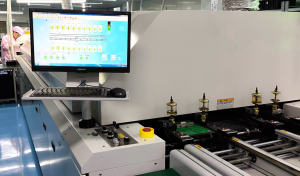
Kingda Custom PCB Assembly Services
Kingda provides PCB manufacturing and assembly support for customers with application-specific circuit board requirements.
Kingda can support custom projects through engineering review, PCB fabrication, component assembly, inspection, and testing according to project specifications.
For custom products, manufacturing requirements should be considered as early as possible. Early DFM review can help identify potential fabrication and assembly issues, while appropriate testing strategies can help verify the finished product.
Whether a project involves a simple rigid PCB, a multilayer board, a flexible circuit, or a more complex assembly, the manufacturing approach should be selected according to the product’s technical and production requirements.
Best Practices for Custom PCB Assembly
For a successful Custom PCB Assembly project, consider the following practices:
- Define electrical and mechanical requirements before PCB design.
- Select PCB materials according to actual operating conditions.
- Consider manufacturing requirements during layout development.
- Conduct DFM analysis before fabrication.
- Confirm the BOM and component availability early.
- Define inspection and testing requirements in advance.
- Validate the prototype before volume production.
- Monitor manufacturing yield during pilot production.
- Maintain revision control for PCB and BOM data.
- Establish clear communication between design and manufacturing teams.
These practices help reduce unnecessary redesigns and improve the transition from engineering development to stable production.
Conclusion
Custom PCB Assembly provides a practical way to develop circuit boards around the specific requirements of an electronic product.
By combining appropriate PCB Design, materials, component selection, manufacturing processes, assembly technologies, inspection, and PCB Testing, engineers can create circuit assemblies optimized for electrical performance, mechanical integration, reliability, and production requirements.
The success of a custom PCB project depends not only on the design itself but also on how effectively the design is translated into a repeatable manufacturing process.
For companies developing specialized electronics, choosing a capable PCB Supplier and involving manufacturing engineering early can help reduce production risks, control costs, and create a smoother path from prototype development to volume manufacturing.