EMI Design on a Microcontroller PCB: Practical Steps
A microcontroller board is a small, self contained design, and that is precisely why EMI design problems are easy to overlook. The clock is internal or driven by a tiny crystal, the currents are modest, and nothing looks like a power stage. Yet the edges are fast, the supply pins are numerous, and the interfaces leave the board through connectors that are far better antennas than any trace. Most microcontroller PCB emissions can be traced to three places: the clock circuit, the decoupling and the I/O.
What Makes a Microcontroller Board Noisy
The noise source is the internal switching of the core and the peripherals, which pulls a rapidly changing current from the supply. That current flows through the package inductance, the board inductance and the decoupling network, and the voltage it develops across them is what couples into the rest of the design. A microcontroller with many pins switching at once is a small, fast current source, and the supply network is the impedance it drives.
The second source is the clock. The crystal layout matters because the oscillator loop is a high impedance node at a precise frequency, and it is sensitive both to disturbance and to layout. A clock trace that is longer than it needs to be, or that runs near a switching node, will carry the disturbance into the timing circuit and can also radiate its harmonics efficiently.

The Crystal and the Clock
Place the crystal as close to the device as the package allows, with the load capacitors adjacent to it and their returns joined to a quiet ground directly beneath the circuit. Keep the loop small, because the oscillator loop carries the circulating current and its area determines how much field escapes. Do not route any other signal through the area between the crystal and the device, and put a ground guard around the circuit where the layout permits.
Where the clock is routed across the board, treat it as a radiator. Keep it short, keep it over a solid reference, and keep it away from the board edge and from connectors. Where an external clock is not required, using the internal oscillator and disabling the external one removes the problem entirely, which is worth considering before the layout is fixed.
Decoupling Around the Device
A microcontroller usually has several supply pins for the core, the I/O and the analogue section, and each group needs its own decoupling. The capacitor belongs against the pin, on the same side of the board where possible, with the return via immediately beside the pad. A capacitor placed a centimetre away with two thin traces is ineffective at the frequencies that matter, no matter what value it carries.
Analogue supply pins deserve separate treatment. They should be fed through a filter, often a ferrite bead with a capacitor on the device side, and referenced to the analogue ground area rather than to the digital return. The filter needs to be placed so that the quiet side stays quiet, which means keeping the noisy supply trace away from it rather than routing it past.
I/O Filtering at the Connector
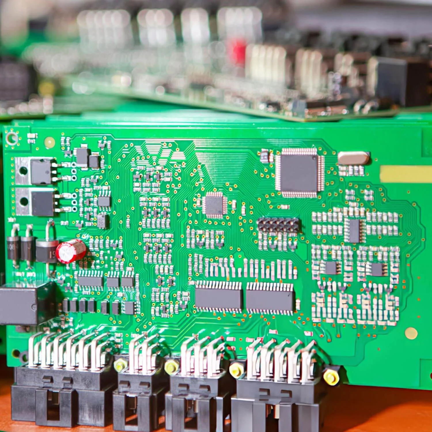
Interfaces are where internal noise becomes external. Any signal that reaches a connector can be carried out onto a cable, and a cable is a far better antenna than a trace. The measures are well established: a series resistor or ferrite bead close to the connector, a capacitor to a quiet reference, and where the signal leaves the enclosure, a transient protection device as well.
Placement decides whether these work. The filter must sit at the connector so that the noisy trace is short and the filtered trace is the long one, and the return from the capacitor must go to a quiet ground rather than to the same copper the interface is trying to escape from. Where several signals share a connector, group their filtering together so that the return paths stay short and common.
Reset, Interrupt and Boot Pins
Reset and interrupt lines are inputs, and they are also long nets that often run from a connector or a switch. They deserve the same treatment as any other susceptible signal: keep them short, keep them away from fast switching nodes, and where they come from off board, filter them at the point of entry. A reset line that picks up a transient will reset the product, and the fault will be attributed to the firmware rather than to the layout.
Boot and configuration pins need attention for a different reason. They are read at power up, so a slow supply ramp combined with a long trace can produce a state that is neither high nor low, and the device enters an unintended mode. Keeping the pull up or pull down close to the pin, and keeping the trace short, removes the ambiguity.
Ground Strategy on a Small Board
A microcontroller board does not need a complicated ground scheme. A single continuous ground plane under the whole design, with the analogue area placed over a region that no digital return current crosses, is the usual answer, and it is more reliable than splitting the plane into islands that must then be joined. The plane gives every signal a return path directly beneath it.
Where an analogue section exists, keep its components and traces in one region and keep the digital return currents out of that region by placement rather than by a split. If a boundary is genuinely needed, make it deliberate and provide a single joining point where the two regions meet. Our notes on mixed signal design guidelines describe where that boundary belongs.
Layout Order for a Microcontroller Design
Place the device first, then the crystal and its capacitors, then the decoupling, then the connectors. That order reflects the priority: the clock circuit is the most sensitive and the most constrained, the decoupling has to be close to the pins, and the connectors are fixed by the mechanics but flexible in their passive components. Routing follows the same order, with the clock loop routed before anything else and the I/O nets routed last so that they can be arranged around the filters.
Keep the ground plane in mind throughout. Every signal should have a reference beneath it, every layer change should have a stitching via, and every via that carries a fast signal should have a return path close by. On a small board with two or four layers, these rules are enough to keep the design quiet. Our notes on EMI control in digital circuits and EMC and EMI control cover the underlying mechanisms.
Verification Without a Chamber
Before investing in a compliance test, a near field probe and a spectrum analyser on a bench will show which part of the board radiates and at which frequencies. Sweeping the probe across a powered board localises the source, and correlating the peaks with the clock harmonics usually identifies it. Comparing the result before and after a change confirms whether the change helped.
The measurement is worth doing on a development board rather than the final article, because the fixes are cheaper earlier. Slowing an edge, restoring a reference, moving a filter to the connector or adding a stitching via are all layout changes, and doing them before the tooling is ordered avoids a revision. Our notes on ground current and harmonic distortion explain how the reference behaviour shows up in the measurement.
FAQ
Does a microcontroller need special EMC treatment? It needs the same fundamentals as any digital design: a continuous reference, correct decoupling, a short clock loop and filtered interfaces. These are cheap measures that remove most of the risk on a small board.
How close should the crystal be? As close as the package and the assembly process allow, with the load capacitors adjacent and their returns joined beneath the circuit. The loop area of the oscillator circuit is what matters.
Is a ferrite bead needed on the analogue supply? It is good practice where the analogue section has its own supply pin. The bead and its capacitor form a filter that keeps digital switching noise out of the analogue reference.