SSD PCB Price Guide: Layer Count, Material and Finish
An SSD board is a small, dense, high-reliability product, and its price reflects all three. A storage drive that loses data when a via cracks or a BGA pad lifts is not acceptable, so the fabrication rules are tighter than the board size suggests. This guide explains how an SSD PCB price is built in 2025, from layer count and materials to via structure, finish and the yield assumptions behind a volume quotation.
What an SSD Board Carries
A solid-state drive board hosts the controller, one to four NAND packages, a power management section and the host connector. The controller is a fine-pitch BGA with a dense escape pattern, the NAND devices are wide bus parts that need matched routing, and the connector fixes the outline. The result is a small board with unusually high routing density.
That density is the reason SSD boards sit at four to eight layers rather than two. The escape routing from the controller alone consumes two signal layers, and the power section needs a plane with low impedance because the current is pulsed. Both requirements are structural, which is why they appear in the price early.
Layer Count and the Price Ladder
Form factor drives the outline as much as the circuit does. A 2280 module is a long narrow board with the connector at one end, so the controller sits close to the connector and the NAND packages are distributed along the length. That arrangement keeps the host interface short, but it leaves very little room for the power section, which is why the power components are usually packed at the far end where the height limit is looser.
Layer count is the clearest step in the price. A 4-layer board is the entry point and suits entry-level drives with a narrow bus and a relaxed thermal limit. A 6-layer board, which is the common configuration for mainstream form factors, adds two internal layers and usually one plane, and it typically costs thirty to fifty percent more than the 4-layer version.
An 8-layer board is used for high-performance drives that need multiple planes, tighter impedance control and better thermal spreading. The increment from six to eight is smaller in percentage than from four to six, because the fabrication process is already at the precision limit and the extra layers are mainly material and lamination time.

Materials: FR-4, High-Tg and Halogen-Free
Standard FR-4 is adequate for a drive that runs cool, but storage products often run warm for long periods, and that is where a high-Tg material earns its cost. Raising the glass transition temperature improves dimensional stability during reflow and reduces the risk of delamination around vias that see repeated thermal cycles.
Halogen-free laminate is a separate specification rather than a performance upgrade, and it is usually requested for products sold into markets with specific material restrictions. It adds a modest amount per board. Choosing between these options should follow the thermal and regulatory requirement rather than the price difference.
Surface Finish and Via Structure
Material choice also affects the assembly process. A laminate with a higher glass transition temperature tolerates a wider reflow window and holds its dimensions through multiple passes, which matters when the drive is assembled on both sides. A cheaper laminate can still work, but the process window narrows and the assembly house may need a tighter profile to compensate, which shifts cost from the board to the line.
An ENIG finish is the usual choice for storage boards. It gives a flat surface for fine-pitch pads, survives multiple reflow cycles and keeps contact resistance stable on the connector. HASL is cheaper but leaves an uneven surface that complicates paste deposition on a 0.4 mm pitch BGA, and OSP has a shelf life that is awkward when assembly is scheduled months after fabrication.
Via structure is the other cost centre. Through-hole vias are cheap and adequate for many nets, while a laser microvia allows escapes that a mechanical drill cannot reach and removes the via stub that degrades a high-speed channel. The trade is that each laser via adds a lamination cycle and a filling step, so it should be used where the routing genuinely needs it.
Prototype, Small Batch and Volume Pricing
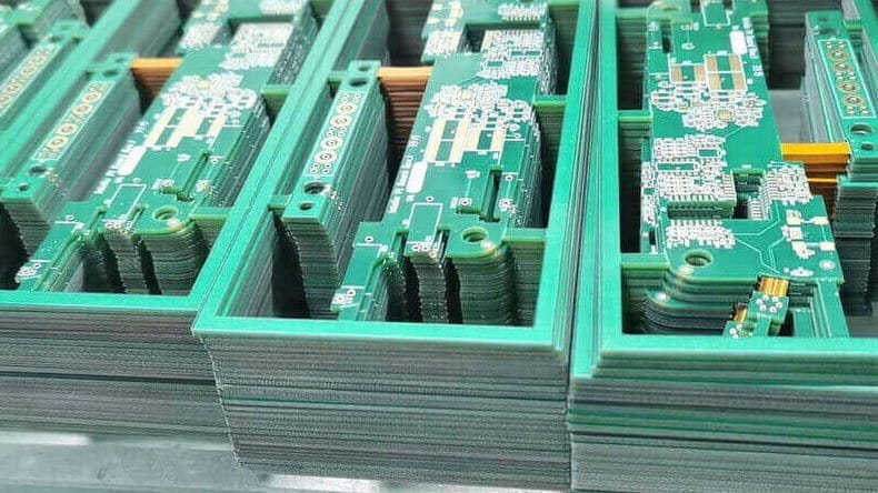
The pcb prototype cost of an SSD board is high per unit because the engineering content is high. A short prototype run carries a stencil, a test programme, an impedance check and often an assembly setup, so the unit price can be three to five times the volume rate. That is not inefficiency; it is the fixed portion of the work being divided by a small number.
Volume pricing then depends on yield. A dense board with a fine-pitch controller and laser vias has a lower yield than a simple 4-layer board, and the fabricator prices that risk into the unit rate. Improving the design for manufacturability is therefore a direct cost reduction, not just a quality exercise.
Regional Pricing and Supply Chain
Regional differences persist at this layer count, but they are smaller than on simple boards because material and process time take a larger share. What remains is the difference in yield expectations, inspection depth and documentation, plus lead time. For a product with a short market window, lead time can outweigh a percentage point of unit price.
Supply chain structure matters too. A drive assembled in one region from boards made in another carries freight, duty and inventory risk, and the cost of carrying safety stock is real. A landed cost comparison that ignores this usually understates the total.
Hidden Costs and Yield Risk
Engineering charges, electrical test, automated optical inspection, X-ray of the BGA area and a first-article report are frequently quoted separately. So are the impedance coupons and the microsection that prove the stackup. Each is a small line item and together they can add a meaningful percentage to a small order.
The largest hidden cost is a bad board. A drive that fails in the field costs a return, a replacement, a shipping charge and often the customer. Applying manufacturable design guidelines before release, and using blind and buried via technology only where the routing requires it, removes most of that risk at almost no cost.
Reducing Cost Without Sacrificing Reliability
Panel utilisation is the first lever, because a small M.2-sized board leaves a lot of panel edge if it is not nested carefully. Improving the panel layout, keeping the outline inside standard dimensions and avoiding an unnecessary finished thickness can reduce the material charge by ten to fifteen percent with no change to the circuit.
The second lever is material discipline: use high-Tg laminate where the thermal requirement justifies it, keep halogen-free only where the market requires it, and reserve laser vias for the nets that cannot be escaped mechanically. The third is order size, since the step from a few hundred to a thousand pieces is the largest single reduction available.
FAQ
Why is an SSD board more expensive than a similar-sized logic board? Density, not size. A fine-pitch controller, a wide NAND bus, impedance control and often laser vias add process steps that a simple board never needs. The small outline actually makes the layout harder because everything has to fit.
Do I need eight layers for a modern drive? Not automatically. A 6-layer stackup serves most mainstream drives. Eight layers become worthwhile when the design needs multiple reference planes, several high-speed channel pairs or significant thermal spreading.
Is ENIG necessary on the connector? It is the safest choice because it stays flat and keeps contact resistance stable. Cheaper finishes can work, but the saving is small relative to the risk of a connector that degrades after storage.