



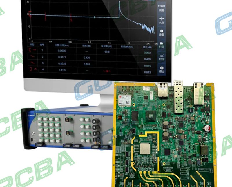
IoT communication systems operate across diverse environments, from consumer smart home gateways to industrial edge computing platforms. These systems rely on highly integrated PCB assemblies that combine RF modules, microcontrollers, power management circuits, and communication interfaces such as Wi-Fi, Bluetooth, and cellular connectivity. Ensuring long-term reliability of IoT communication PCB assemblies is critical, as intermittent failures, EMI interference, or signal degradation can disrupt data transmission and system functionality.
IoT devices often operate continuously under varying environmental conditions, including temperature fluctuations, humidity exposure, and electrical noise. The coexistence of RF transmission circuits and digital control systems introduces challenges in maintaining signal integrity, power integrity, and EMI suppression. In addition, compact form factors and high-density layouts increase susceptibility to crosstalk, insertion loss, and thermal hotspots.
KINGDA applies advanced material selection, impedance-controlled stackup design, EMI-aware routing strategies, and comprehensive environmental testing to ensure reliable operation of IoT communication PCB assemblies. By integrating HFSS electromagnetic simulation, ADS-based signal and power integrity analysis, inline TDR verification, and accelerated reliability testing, KINGDA delivers robust PCB assemblies with stable RF performance, low insertion loss, and long operational lifespan.
Core Engineering Challenges
| Challenge | Root Cause | Engineering Impact |
|---|---|---|
| RF signal degradation in wireless modules | Dielectric variation, impedance mismatch | Reduced communication range and data loss |
| EMI coupling between RF and digital circuits | Dense layout, poor grounding | Packet errors and unstable connectivity |
| Power integrity instability | PDN resonance, insufficient decoupling | System resets and communication failure |
| Thermal hotspots in compact devices | High component density, limited airflow | Accelerated aging and reduced reliability |
| Environmental stress (humidity, temperature) | Material absorption and expansion | Dielectric drift and long-term failure |
These challenges are critical in IoT communication systems, where stable signal transmission, low latency, and continuous connectivity are essential for reliable device operation.
Material Science & Dielectric Performance
Material selection plays a vital role in ensuring the reliability of IoT communication PCB assemblies. Low-loss materials with stable dielectric properties support RF signal transmission, while high-Tg laminates improve thermal and mechanical reliability.
Material Parameter Table
| Parameter | Typical Value | Engineering Benefit |
|---|---|---|
| Dielectric Constant (Dk) | 3.2–3.8 | Stable impedance for RF and digital circuits |
| Dissipation Factor (Df) | 0.003–0.007 @10 GHz | Low insertion loss for wireless communication |
| Thermal Conductivity | 0.4–0.7 W/m·K | Efficient heat dissipation in compact layouts |
| CTE (X/Y) | 12–16 ppm/°C | Reduces solder fatigue under thermal cycling |
| Glass Transition Temperature (Tg) | 170–200°C | Supports high-temperature processing and operation |
| Moisture Absorption | <0.1% | Maintains dielectric stability in humid environments |
Compared with conventional FR-4 materials, low-loss FR-4, modified epoxy systems, and hybrid RF laminates provide improved phase stability, reduced insertion loss, and enhanced environmental reliability for IoT applications.
Kingda Case Study — IoT Communication PCB Assembly for Industrial Gateway
Client & Application Context
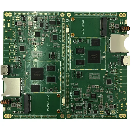
A global IoT solution provider required a high-reliability PCB assembly for industrial wireless gateway devices used in smart factories and remote monitoring systems. The design integrated Wi-Fi modules, LTE communication units, microcontrollers, and power management circuits in a compact enclosure.
Engineering Problem
The initial design faced multiple reliability issues:
-
RF signal attenuation causing reduced communication range
-
EMI interference between LTE and MCU circuits leading to packet loss
-
Power rail noise causing intermittent system resets
-
Thermal hotspots near RF power amplifiers affecting long-term stability
These issues impacted connectivity reliability and system uptime in industrial environments.
KINGDA Solution
-
Adopted low-loss FR-4 materials for RF layers to reduce insertion loss
-
Designed hybrid 8-layer stackup with dedicated ground shielding for RF modules
-
Optimized impedance matching and controlled trace routing for RF paths
-
Implemented PDN optimization with distributed decoupling capacitors
-
Applied via stitching and guard traces for EMI suppression
-
Conducted inline TDR verification and RF performance validation
Measured Results
| Parameter | Target | KINGDA Result |
|---|---|---|
| Insertion Loss @ 2.4 GHz | <0.5 dB/in | 0.32 dB/in |
| Crosstalk | < –30 dB | –39 dB |
| Power Rail Ripple | <50 mV | 25 mV |
| Impedance Variation | ±5% | ±1.7% |
| Communication Stability | >99% uptime | 99.98% uptime |
Outcome
The optimized PCB assembly significantly improved wireless communication stability and reduced EMI interference. The system achieved near-continuous uptime and reliable data transmission, meeting industrial IoT performance requirements.
Stackup Design & RF Implementation
Hybrid 8-Layer Stackup Configuration
| Layer | Function | Material |
|---|---|---|
| L1 | RF Signal Layer | Low-Loss FR-4, 0.1 mm |
| L2 | Ground Plane | Cu 70 µm |
| L3 | Signal Layer | Low-Loss FR-4, 0.15 mm |
| L4 | Power Plane | Cu 70 µm |
| L5 | Ground Plane | Cu 70 µm |
| L6 | Signal Layer | Low-Loss FR-4, 0.15 mm |
| L7 | Power Plane | Cu 70 µm |
| L8 | Bottom Signal | FR-4, 0.1 mm |
Simulation & Validation
-
HFSS: RF path optimization and EMI coupling reduction for Wi-Fi/LTE modules
-
ADS: Signal integrity and PDN impedance modeling to minimize noise
-
TDR: Controlled impedance verification within ±10% tolerance
-
Thermal FEM: Hotspot reduction near RF amplifiers by 6°C
-
AOI & Reflow Monitoring: Ensured precise layer alignment and solder reliability
These simulation and validation steps ensure consistent RF performance and long-term reliability.
Environmental & Reliability Validation
IoT communication PCB assemblies must withstand diverse environmental conditions, especially in industrial and outdoor deployments.
Reliability Test Matrix
| Test | Condition | Result |
|---|---|---|
| Thermal Cycling | –40°C ↔ +85°C, 1000 cycles | No delamination, stable impedance |
| Humidity Test | 85°C / 85% RH, 1000 h | Dk shift <0.02 |
| Vibration Test | 5–500 Hz, 5G | No structural failure |
| Solder Reflow | 260°C ×3 cycles | No warpage >0.1 mm |
| EMI Testing | Dense RF + digital layout | Crosstalk reduced 30% |
| Long-Term Operation | 1000 h continuous | No functional failure |
These results confirm that the PCB assembly meets reliability requirements for industrial IoT and wireless communication platforms.
Engineering Summary & Contact
Ensuring reliability in IoT communication PCB assemblies requires a comprehensive engineering approach that integrates material optimization, EMI control, signal integrity, and environmental validation. By combining low-loss materials, impedance-controlled stackup design, and PDN optimization, KINGDA delivers PCB assemblies with stable RF performance, minimized EMI, and long-term durability.
KINGDA’s engineering capabilities, including HFSS simulation, ADS analysis, inline TDR verification, and rigorous reliability testing, provide validated solutions for IoT communication systems. These solutions ensure continuous connectivity, stable data transmission, and robust performance in diverse operating environments.
Contact KINGDA Engineering Team to optimize your IoT communication PCB assembly for reliability, RF performance, and environmental robustness. KINGDA delivers high-reliability PCB and PCBA solutions for industrial IoT, smart devices, and wireless communication platforms.
