Even Layer Count in PCB Stackups: Why Boards Avoid Odd Layers
Ask a fabricator why almost every multilayer board has an even number of layers and the honest answer is that odd ones are possible but rarely worth the trouble. The even layer count is not a rule of physics; it is the result of how panels are built up from cores and prepreg, and of what happens to a stack that is not mechanically symmetrical.
Why Odd Counts Are Rare in Practice
A multilayer board is assembled from cores, which are rigid pieces of laminate with copper on both faces, and prepreg, which is partially cured resin used as the adhesive between them. A signal layer on the outside of the stack has to be bonded with prepreg; a core always contributes two copper layers at once. The arithmetic of that construction naturally produces even numbers, and an odd count forces one more foil layer onto one side, which is exactly where the symmetry is lost.
Most four-layer and six-layer boards are built this way, and the same logic extends up to the highest layer counts, which is why the industry quotes 8, 12 and 20 rather than 9, 13 and 21.
The Cost Argument
Odd-layer boards are not cheaper. It is true that an odd stack uses one less layer of material and one less sheet of copper foil, so the raw material cost is slightly lower. That saving is more than offset by the extra processing: the additional foil layer has to be laminated onto a core, which cannot be done in the same press cycle as the rest of the stack, and the surface that results from that extra bonding step needs additional preparation before it can be imaged and etched.

Every extra handling step is another opportunity for a scratch, an etch defect or a registration error, so the yield penalty shows up quickly on fine-line designs.
Warpage and Balanced Construction
The real argument is mechanical. After lamination the board cools from pressing temperature to room temperature, and every layer shrinks by an amount set by its copper coverage and its resin content. In a symmetrical stack the contraction on either side of the centre line cancels, and the board stays flat. In an asymmetrical stack, one side contracts more than the other and the board bows.
Bowing is not only cosmetic. A warped board cannot be printed with paste evenly, cannot be placed accurately, and will not sit flat in a reflow oven, so the assembly yield suffers even where the bare board passes inspection.
What Lamination Does to an Unbalanced Stack
The mechanism is worth stating plainly. Copper and resin have very different coefficients of thermal expansion, and the effective contraction of a layer depends on how much copper is on it. Where the copper distribution on one side of the stack does not match the other, the difference is locked in by the cured resin and can only be released by heat, which is why a board that looks flat at inspection can bow when it passes through reflow.
The remedy for an odd count is usually a balanced construction: add a dummy layer, or use a heavier copper foil on the side that needs stiffening, so that the two halves of the stack match. Balanced stackups and odd layer counts describes how the two approaches compare.
The Warpage Limit
The applicable standard sets a flatness limit that is normally expressed as a percentage of the diagonal. Around 0.7 percent is the figure commonly quoted for surface-mount boards, measured after the board has been through the thermal excursion the assembly process will apply. A three-layer board of any significant size has trouble meeting that figure, while the equivalent four-layer stack usually meets it without special measures.
Ask for the measurement, not the intention. A fabricator who can show warpage data on the actual stackup is worth more than a promise that the board will be flat.
Fake Even Builds: Designing Five as Six
The usual compromise is to design the function on an odd count and fabricate it on the next even number. A five-layer requirement becomes six layers with one layer used as an extra reference plane; a seven-layer design becomes eight. The additional layer is not wasted, because an extra ground or power plane reduces the impedance of the return path and improves the electrical behaviour of the stack.
The alternative is to build the odd stack as a foil construction, where an extra copper foil is bonded to one side after the main lamination. This works and is used for a minority of boards, but it costs more, and the asymmetric construction means the warpage risk is never fully removed. Where the layer count must be odd for mechanical reasons — a total thickness limit, for example — this is the route to take, and the trade-off should be discussed with the fabricator before the stackup is fixed.
Process and Handling Penalties
Beyond warpage, an odd stack brings everyday manufacturing friction. The asymmetric build is harder to handle in the lamination press, harder to register during drilling, and harder to keep clean during the extra bonding step. The panel is also more likely to need an additional bake before assembly, which adds cycle time. None of these individually is fatal, and together they explain why designers default to even numbers.
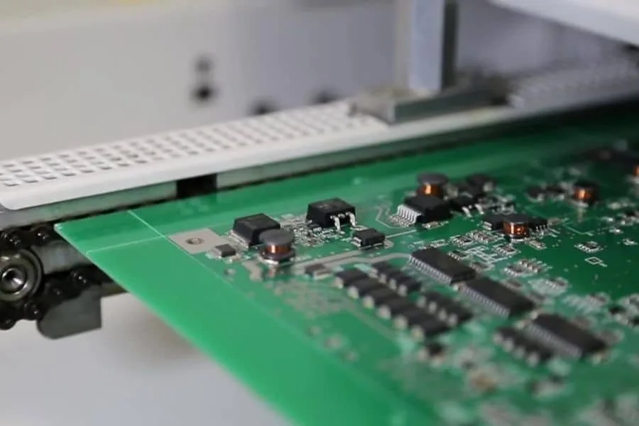
<img src="https://www.gopcba.com/wp-content/uploads/2026/08/A-close-up-view-of-a-machine-producing-a-bright-light-768×511-1.webp" alt="warpage risk in an unbalanced lamination of an odd layer stackup” />
Documentation matters more on these builds as well. An odd layer stackup has to be drawn explicitly, with the foil construction, the prepreg types and the copper weights stated for each interface, because the fabricator cannot infer the intent from the layer count alone. When the drawing is ambiguous, the shop will choose the construction that is easiest to press, and that choice may not be the one the electrical design assumed.
For a design that is being released to production, the practical advice is straightforward: lay the stackup out in pairs of layers, place the reference planes symmetrically, and let the layer count land on an even number. Layer stackup design covers the pairing rules for common layer counts.
When an Odd Count Is Justified
There are cases where an odd layer stackup is the right answer. A thick copper layer for a high-current rail may make the stack symmetrical without adding a plane, and a flex or rigid-flex construction may be constrained by bend radius and total thickness rather than by warpage. In those cases the stack can be balanced by adjusting copper weights rather than layer count, which achieves the same mechanical result. The test to apply is simple: if the two halves of the stack contract by the same amount when the resin cools, the count does not matter.
A rigid-flex board with a single heavy copper layer on one side is a good example: the copper weight and the dielectric thickness are chosen so that the two halves contract equally, and the board stays flat without a dummy layer. PCB dimensional stability explains how those coefficients are measured.
FAQ
Are odd-layer boards impossible to make? No, they are made regularly. They cost more and carry more warpage risk, which is why they are avoided when an even stack can do the same job.
Does adding a layer to make the count even change the impedance? It can, if the new layer changes the dielectric thickness above a signal layer. If the extra layer is added as a plane in a position that preserves the existing distances, the controlled impedances stay as designed.
What warpage figure should be specified? Around 0.7 percent of the diagonal is a common requirement for surface-mount assembly. Specify it after the thermal excursion the board will see, not at room temperature.