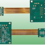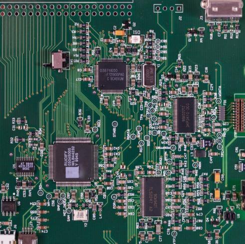
With the rapid development of electronic communication technology, traditional PCB Manufacturing methods must continually evolve to meet the demands of modern electronic products. Today’s devices require smaller dimensions, higher circuit density, improved electrical performance, and shorter development cycles.
For engineers, shortening the time between PCB Design completion and a functional prototype can significantly accelerate product development. This has led to the increasing importance of Fast PCB Prototyping and other rapid PCB Prototyping techniques.
Rapid prototyping is particularly useful during the early stages of product development, when engineers need to verify circuit functionality, component placement, routing, electrical performance, and mechanical compatibility before moving into mass production.
1. Common Methods for Fast PCB Prototyping
There are many approaches to producing a PCB prototype. In general, rapid circuit-board fabrication methods can be divided into two broad categories: mechanical processes and chemical or photographic processes.
Mechanical PCB Fabrication
Mechanical methods use cutting, milling, engraving, or other machining tools to remove unwanted copper from a copper-clad laminate.
In a basic prototype, a milling machine or CNC router can selectively remove copper according to the circuit pattern. This approach avoids chemical etching and can be useful when only a small number of prototypes are required.
However, mechanical fabrication has limitations. The achievable trace width and spacing depend heavily on tool diameter, machine accuracy, spindle stability, board flatness, and process control. Fine-pitch and high-density circuits can therefore be difficult to manufacture using basic mechanical engraving.
Mechanical prototyping is more suitable for relatively simple circuits, quick engineering verification, and applications where manufacturing speed is more important than extremely fine geometries.
Chemical and Photographic PCB Fabrication
Chemical processes form the circuit pattern by protecting the copper that needs to remain and removing unwanted copper through etching.
Several pattern-transfer techniques can be used for prototype fabrication, including:
- Manual pattern drawing
- Adhesive or transfer-film methods
- Photoresist imaging
- Toner or thermal-transfer methods
- Computer-controlled imaging processes
Among these approaches, photographic imaging provides significantly better pattern consistency and is more suitable for fine circuit features.
2. Manual Pattern Drawing
One of the simplest prototype techniques is manually drawing the required circuit pattern onto a copper-clad board using an etch-resistant material.
After the protective pattern has been applied, the board is exposed to an etching solution. The unprotected copper is removed while the protected areas remain as conductive traces.
Although this method is inexpensive and easy to understand, it has significant limitations in accuracy and repeatability. It is generally suitable only for simple prototype circuits rather than modern high-density PCB designs.
For professional PCB Fabrication, computer-generated artwork and controlled imaging processes provide much more consistent results.
3. Adhesive and Transfer-Film Methods
Another basic prototyping approach uses pre-cut adhesive shapes, transfer films, or other pattern-transfer materials.
Different shapes can be combined on the copper surface to define the desired circuit pattern. After the pattern is firmly attached, the board can be etched.
This method eliminates some of the drawing work associated with manual fabrication, but the final accuracy still depends on the quality of the transfer material and the precision with which it is applied.
It becomes increasingly difficult to use this approach for fine-pitch components, narrow trace spacing, dense vias, and complex multilayer designs.
4. Photoresist Imaging
Photoresist technology is a more advanced approach to rapid PCB fabrication.
A photosensitive resist is applied to the copper-clad laminate and exposed using an appropriate artwork or imaging system. During development, selected areas of the resist are removed or retained according to the resist type and imaging process.
The resulting pattern protects the required copper areas during etching.
In professional PCB production, imaging processes are highly controlled to achieve accurate trace geometry and registration. Modern PCB factories may use direct imaging or other automated exposure technologies rather than relying on basic film-based methods.
Photoresist imaging is particularly useful when the prototype requires more accurate traces and spaces than can be achieved with manual methods.
5. Thermal Transfer Prototyping
Thermal-transfer methods use heat to transfer a printed circuit pattern onto a copper-clad laminate.
The transferred material acts as an etch-resistant layer. After transfer, the exposed copper is removed during the etching process.
This technique can be relatively inexpensive for basic prototypes, but its accuracy depends on the printer, transfer medium, temperature, pressure, surface preparation, and transfer quality.
It is therefore better suited to simple engineering prototypes than to high-density production PCBs.
6. Advantages and Limitations of Rapid PCB Prototyping
Rapid PCB Prototyping provides an effective way to verify circuit concepts before committing to production tooling and large-scale manufacturing.
Its major advantages include:
- Shorter prototype development cycles
- Lower initial development cost
- Faster functional verification
- Easier design iteration
- Early detection of PCB design problems
- Reduced risk before mass production
However, rapid prototyping methods also have limitations. Prototype processes that are suitable for simple boards may not reproduce the same performance, reliability, or dimensional accuracy as professional PCB Manufacturing processes.
Therefore, engineers should distinguish between a board made for basic functional verification and a production-qualified PCB.
7. Major Challenges in Rapid PCB Prototyping
7.1 Printing and Pattern Accuracy
When printed or transferred artwork is used, the quality of the pattern directly affects the final PCB.
Insufficient resolution can result in:
- Uneven trace widths
- Open circuits
- Short circuits
- Inadequate pad dimensions
- Poor edge definition
As trace width and spacing become smaller, pattern-transfer accuracy becomes increasingly important.
7.2 Photoresist Exposure and Development
Photoresist-based processes require appropriate exposure and development conditions.
Exposure time is not a universal fixed value. It depends on the resist material, thickness, exposure source, artwork, equipment, and process conditions.
Insufficient exposure or development can cause incomplete pattern formation, while excessive exposure may affect feature definition.
Professional manufacturers therefore establish process windows through controlled testing rather than relying on a single fixed exposure time.
7.3 Etching Control
PCB Etching is one of the most critical steps in subtractive circuit fabrication.
Etching quality is affected by factors such as:
- Etchant chemistry
- Temperature
- Concentration
- Spray or immersion conditions
- Etching time
- Copper thickness
- Circuit geometry
- Equipment condition
If etching is excessive, conductor widths can become smaller than intended. If etching is insufficient, unwanted copper may remain and create shorts.
This phenomenon is commonly associated with undercutting, where the etchant removes copper not only vertically but also laterally beneath the resist.
Professional PCB Fabrication therefore requires controlled etching parameters and process monitoring.
7.4 Environmental and Waste-Treatment Requirements
Chemical-based prototyping produces waste solutions containing dissolved copper and other process chemicals.
In professional manufacturing environments, wastewater and chemical waste must be collected, treated, and managed according to applicable environmental regulations.
This is one reason why laboratory-scale etching and professional Circuit Board Manufacturing should not be treated as equivalent processes.
7.5 Drilling and Mechanical Processing
After etching, prototype boards may require holes for through-hole components, mounting hardware, or vias.
Manual drilling can introduce positional errors, especially when the design contains a large number of small holes or fine-pitch components.
Professional PCB manufacturers use controlled drilling equipment and manufacturing data to achieve much higher positional accuracy and repeatability.
8. Rapid Prototyping vs. Professional PCB Manufacturing
Rapid prototype methods are useful during the engineering verification stage, but they cannot always replace professional PCB Manufacturing.
A professional manufacturing process may include:
- Engineering and CAM data preparation
- Material selection
- Inner-layer imaging
- Etching
- Lamination
- CNC or laser drilling
- Desmear and hole preparation
- Copper plating
- Outer-layer imaging and etching
- Solder mask application
- Surface finishing
- Electrical testing
- Final inspection
These controlled processes allow manufacturers to achieve much higher levels of dimensional accuracy, electrical performance, reliability, and production consistency.
For multilayer, HDI, high-speed, or fine-pitch designs, professional fabrication is generally essential.
9. How PCB Design Affects Prototype Speed
The speed of Fast PCB Prototyping is not determined only by manufacturing equipment. PCB design quality also has a significant influence on the overall development cycle.
A design that follows design-for-manufacturing principles can reduce unnecessary revisions and improve prototype success rates.
Important considerations include:
Trace Width and Spacing
Trace width and spacing should be selected according to electrical requirements and the manufacturer’s actual process capability.
Via and Hole Design
Via diameter, drill size, aspect ratio, annular ring, and spacing should be compatible with the selected manufacturing process.
Layer Stackup
For multilayer and high-speed designs, the stackup should be established early. Signal layers, power planes, ground planes, dielectric thickness, and controlled-impedance structures all influence PCB performance.
Component Placement
Good component placement can simplify routing, reduce unnecessary trace length, and improve assembly efficiency.
DFM Review
A Design for Manufacturing review can identify potential issues before fabrication, reducing the probability of prototype failure and repeated manufacturing cycles.
10. Choosing the Right Rapid PCB Prototyping Method
The appropriate prototyping method depends on the complexity and purpose of the board.
For simple single-sided circuits, basic mechanical or chemical methods may be sufficient for functional verification.
For more complex boards, photoresist imaging or professional rapid PCB Fabrication provides better control over circuit geometry.
For multilayer, HDI, high-speed, RF, automotive, medical, or other reliability-sensitive applications, engineers should generally work with an experienced PCB manufacturer from the beginning rather than relying on simplified laboratory fabrication techniques.
The prototype should reproduce the important characteristics of the intended production board whenever possible. Otherwise, a prototype may function correctly at a basic level while failing to represent production-level electrical or mechanical performance.
11. Kingda’s Rapid PCB Prototyping Support
At Kingda, rapid PCB development is supported through coordinated engineering and manufacturing processes designed to shorten the transition from PCB Design to functional prototype.
A professional prototype process should consider not only fabrication speed but also material selection, stackup design, manufacturability, electrical requirements, inspection, and the eventual transition to volume production.
By evaluating these factors early, Kingda can help customers identify potential manufacturing risks, optimize PCB designs, and establish a smoother path from prototype verification to production.
Conclusion
The development of modern electronic products requires increasingly fast and reliable PCB development cycles. Fast PCB Prototyping allows engineers to verify circuit concepts, identify design problems, and make improvements before entering full-scale production.
Mechanical engraving, chemical etching, photoresist imaging, and thermal-transfer techniques can all be used for different types of prototypes. However, their achievable accuracy, repeatability, and reliability vary considerably.
For simple functional verification, basic prototyping methods may be sufficient. For complex, high-density, high-speed, or reliability-critical designs, professional PCB Manufacturing and controlled PCB Fabrication processes are essential.
Ultimately, successful rapid PCB development depends on the combination of sound PCB Design, appropriate prototyping technology, accurate manufacturing data, and close cooperation between engineers and the PCB manufacturer.