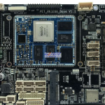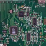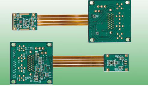
HDI PCB stands for High-Density Interconnect PCB. High-Density Interconnect technology is an advanced PCB Manufacturing technology developed to accommodate the increasing demands for miniaturization, higher component density, faster signal transmission, and greater functionality in modern electronic products.
A printed circuit board is a structural platform composed of insulating materials and conductive patterns. During final assembly, integrated circuits, transistors, diodes, passive components such as resistors and capacitors, connectors, and other electronic devices are mounted onto the board. The conductive patterns and interconnection structures provide electrical connections between these components, allowing the complete electronic system to perform its intended functions.
Therefore, a PCB is not simply a collection of copper traces. It is a critical platform that provides mechanical support, electrical interconnection, power distribution, signal transmission, and, depending on the design, thermal management for electronic components.
Understanding HDI and Printed Circuit Boards
Because a PCB is generally an intermediate component rather than a complete end product, its terminology can sometimes be confused with that of other electronic assemblies.
For example, a computer motherboard contains a complex PCB structure, but a motherboard and a PCB are not technically identical concepts. Similarly, an IC substrate is designed specifically for high-density interconnection between semiconductor packages and system-level circuitry and should not simply be treated as a conventional PCB.
As electronic products become increasingly multifunctional and sophisticated, the pitch between component connections continues to decrease while signal transmission speeds increase. These trends require more interconnections within a smaller physical area.
Traditional PCB structures can eventually reach their practical limits when designers need to accommodate fine-pitch components, large numbers of signal connections, and strict mechanical size constraints. This is one of the major reasons why High-Density Interconnect technology has become increasingly important.
Why HDI PCB Technology Is Needed
Early electronic products could often be implemented using single-sided or double-sided PCBs. However, as circuit complexity increased, it became increasingly difficult to route all required signals on only two conductive layers.
Multilayer structures provided additional signal, power, and ground layers, making it possible to accommodate more connections within a limited board area. However, simply adding more layers does not always provide the most efficient solution.
Conventional through-hole vias extend through the entire PCB thickness. When a board contains a large number of through-holes, these vias can consume valuable routing space on multiple layers.
HDI PCB technology addresses this limitation by using smaller interconnection structures, particularly Microvias, blind vias, and build-up layers. These structures allow designers to create shorter and more localized electrical connections while improving routing density.
The benefits can include:
- Higher wiring density
- Smaller PCB dimensions
- More efficient use of board area
- Better support for fine-pitch components
- Shorter electrical interconnection paths
- Improved routing flexibility
- Greater integration of power and signal structures
- Support for compact and lightweight electronic products
HDI PCB and High-Speed Signal Transmission
Modern electronic systems increasingly operate at high data rates. As signal frequencies and edge rates increase, PCB design must address signal integrity, power integrity, electromagnetic interference, and impedance control.
A high-speed PCB may require controlled impedance structures such as microstrip and stripline routing. Multilayer stackups with carefully designed reference planes are commonly used to establish predictable return-current paths and reduce unwanted electromagnetic coupling.
For high-speed applications, HDI Manufacturing can provide additional design flexibility by enabling shorter interconnections and smaller via structures. Shorter signal paths can help reduce parasitic effects, although actual electrical performance depends on the complete stackup, material properties, routing geometry, via structure, and operating frequency.
PCB materials also become increasingly important as transmission speed increases. Materials with suitable dielectric constant (Dk), dissipation factor (Df), thermal properties, and dimensional stability may be selected according to the application.
Therefore, HDI should not be considered only a method for making smaller holes. It is an overall interconnection technology that integrates material selection, layer stackup, microvia formation, fine-line routing, registration control, plating, and manufacturing process control.
What Are Microvias?
One of the defining characteristics of an HDI PCB is the use of Microvias.
A microvia is a very small via typically formed by laser drilling and used to connect adjacent or nearby conductive layers. Industry definitions and manufacturing classifications can vary, but microvias are generally associated with very small-diameter structures, often around or below 150 μm.
Compared with conventional through-hole vias, microvias can occupy significantly less routing space. This allows designers to place interconnections closer to fine-pitch component pads and create more compact routing structures.
Microvias can be implemented in several configurations, including:
- Blind microvias connecting an outer layer to an internal layer
- Stacked microvias positioned vertically across multiple build-up layers
- Staggered microvias offset between adjacent layers
- Microvias integrated with fine-pitch BGA escape routing
The selection of a particular microvia structure depends on PCB thickness, layer count, component pitch, reliability requirements, manufacturing capability, and cost considerations.
Build-Up PCB Technology
The development of Build-Up PCB structures has played an important role in the evolution of HDI technology.
In a conventional multilayer PCB, multiple copper layers and dielectric layers are laminated together before through-hole drilling and plating. In a build-up structure, additional dielectric and copper layers are sequentially formed around a core structure.
This approach enables microvias to be created between specific adjacent layers rather than requiring a hole to pass through the entire board.
A simplified build-up structure may include:
Core → dielectric layer → copper layer → microvia → additional dielectric/copper layers
This process can be repeated on one or both sides of the core depending on the required HDI structure.
Build-up technology provides greater flexibility for high-density routing and is particularly useful for applications involving fine-pitch BGA, CSP, advanced processors, mobile devices, medical electronics, automotive electronics, and other compact electronic systems.
Different Names for HDI Technology
As high-density interconnection technology developed, different regions and manufacturers used different terms to describe similar or related structures.
Some manufacturers and industry documents have used SBU (Sequential Build-Up) to describe sequentially constructed PCB structures. The term emphasizes the manufacturing approach in which additional layers are built up sequentially.
The term Microvia Process (MVP) has also been used to emphasize the use of microvia technology.
Another term, Build-Up Multilayer Board (BUM), describes multilayer PCBs manufactured using build-up structures. Traditional multilayer boards are commonly referred to as MLBs.
Although these terms can describe specific structures or manufacturing approaches, High-Density Interconnect has become the widely recognized general terminology for this category of PCB technology.
HDI PCB Manufacturing Process
Producing an HDI PCB requires tighter process control than many conventional PCB structures. Depending on the design, the manufacturing process may include several specialized steps.
1. CAM and Engineering Preparation
Manufacturing begins with engineering data review, CAM processing, stackup verification, design-rule analysis, and manufacturability evaluation.
Important factors include:
- Layer structure
- Microvia diameter and depth
- Trace width and spacing
- Pad dimensions
- Registration requirements
- Copper thickness
- Material selection
- Sequential lamination structure
Early DFM analysis can help identify potential manufacturing risks before production begins.
2. Laser Drilling
Laser drilling is widely used to form microvias in HDI structures.
Depending on the dielectric material and construction, different laser technologies may be selected. CO₂ and UV laser systems are among the technologies used in PCB manufacturing, with process selection depending on material properties and hole requirements.
Laser parameters must be carefully controlled to achieve consistent hole geometry without excessive damage to surrounding materials.
3. Desmear and Hole Preparation
After drilling, residues and resin material may remain inside the microvia. Desmear and cleaning processes are therefore used to prepare the hole surface for reliable metallization.
The objective is to establish a clean and suitable surface for subsequent copper deposition while maintaining the required hole geometry.
4. Copper Plating
Copper plating forms the conductive connection between layers.
Because HDI structures often involve small microvias and fine features, plating uniformity is particularly important. Poor plating control can result in insufficient copper coverage, voids, cracks, or reliability problems.
5. Sequential Lamination
For advanced HDI Manufacturing, sequential lamination may be used to construct additional build-up layers.
The lamination process must control temperature, pressure, resin flow, layer registration, material thickness, and dimensional stability. Accurate registration is especially important because the cumulative alignment tolerance becomes more challenging as additional build-up cycles are introduced.
6. Fine-Line Circuit Formation
HDI designs often require finer traces and spaces than conventional PCBs.
Etching performance, copper thickness, imaging accuracy, exposure control, and process compensation all influence the final conductor geometry.
Manufacturing capability should therefore be evaluated using the actual material stackup and production process rather than relying only on nominal design values.
HDI PCB and Fine-Pitch Components
The development of component packaging has been another major driver behind HDI technology.
Packages such as BGA and CSP significantly increase the number of electrical connections within a relatively small area. Conventional through-hole structures may not provide sufficient routing flexibility for these packages.
HDI structures allow designers to route signals from fine-pitch component pads through microvias and build-up layers. This makes it easier to escape dense BGA patterns and distribute signals to internal layers.
As component pitch continues to decrease, the relationship between package design and HDI PCB manufacturing capability becomes increasingly important.
HDI PCB Design Considerations
Successful HDI design requires close cooperation between PCB designers and manufacturers.
Important considerations include:
Microvia Structure
The diameter, depth, aspect ratio, stacking method, and landing-pad design of microvias must be compatible with the manufacturer’s process capability.
Stackup Design
The stackup should provide appropriate signal-reference relationships, power distribution, impedance control, and mechanical balance.
Registration Accuracy
High-density structures have limited tolerance for layer misalignment. Registration control becomes especially important for sequential lamination and fine-pitch component interfaces.
Signal Integrity
High-speed signals should be routed with appropriate reference planes, controlled impedance, suitable via structures, and well-defined return-current paths.
Thermal and Mechanical Reliability
As the number of layers and build-up cycles increases, designers should also consider thermal expansion, Z-axis movement, copper distribution, board warpage, and long-term reliability.
Applications of HDI PCBs
High-Density Interconnect technology is widely used in electronic products where space, routing density, and electrical performance are important.
Typical applications include:
- Smartphones and tablets
- Wearable electronics
- High-performance computing systems
- Networking and communication equipment
- Automotive electronics
- ADAS and automotive control systems
- Medical electronics
- Industrial control equipment
- Consumer electronics
- Compact IoT devices
The exact HDI structure varies according to the application’s electrical, mechanical, thermal, and reliability requirements.
HDI PCB vs. Conventional Multilayer PCB
The main difference between an HDI structure and a conventional Multilayer PCB is not simply the number of layers.
A conventional multilayer board may primarily rely on through-hole vias for interconnection. An HDI design typically combines fine-line circuitry, microvias, blind vias, build-up layers, and high-accuracy registration to achieve higher interconnection density.
In other words, HDI is better understood as an advanced interconnection architecture rather than merely a high-layer-count PCB.
A properly engineered HDI design can sometimes achieve the required routing density with fewer overall layers than a conventional approach, although the actual result depends heavily on the circuit design and stackup.
Quality Control in HDI Manufacturing
Because HDI structures contain extremely small features, manufacturing consistency is critical.
Key quality-control areas include:
- Microvia geometry
- Copper plating thickness
- Microvia integrity
- Interlayer registration
- Trace width and spacing
- Surface copper distribution
- Lamination quality
- Material dimensional stability
- Impedance control
- Electrical continuity and isolation
- AOI and other inspection processes
- Reliability testing where required
Advanced inspection and process monitoring can help manufacturers identify defects before they affect final assembly.
Kingda’s Approach to HDI PCB Manufacturing
At Kingda, HDI production is approached as an integrated engineering and manufacturing process rather than simply a microvia drilling operation.
The key is to coordinate HDI PCB design requirements with material selection, stackup engineering, laser drilling, sequential lamination, copper plating, fine-line fabrication, registration control, inspection, and electrical testing.
For customers developing compact, high-density electronic products, Kingda can evaluate the relationship between PCB design and manufacturing capability at an early stage. This helps identify potential DFM issues, optimize the stackup, select appropriate interconnection structures, and improve manufacturing reliability.
As electronic products continue to become smaller, faster, and more integrated, HDI Manufacturing will remain an important technology for achieving higher interconnection density without continuously increasing PCB size.
Conclusion
HDI PCB technology was developed in response to the increasing demand for miniaturization, high-density routing, fine-pitch components, and high-speed electrical performance.
Through Microvias, sequential build-up structures, fine-line circuitry, and high-precision manufacturing processes, HDI technology enables designers to create compact and highly integrated electronic systems.
However, achieving reliable HDI performance requires more than simply reducing via size. Stackup design, material selection, signal integrity, registration accuracy, plating quality, lamination control, and manufacturing tolerances must all work together.
For this reason, close cooperation between PCB designers and an experienced PCB Manufacturing partner is essential for achieving a reliable, manufacturable, and cost-effective HDI solution.