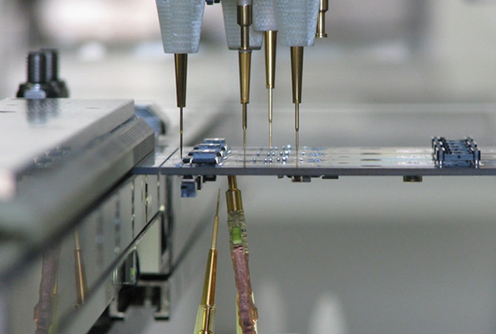
Flying Probe Testing is an advanced PCB Testing method developed to address the limitations of conventional electrical testing, particularly for prototypes, small-batch production, and complex high-density circuit boards. Instead of using a fixed bed-of-nails fixture, a flying probe tester uses multiple motor-driven probes that move rapidly and precisely across the PCB surface to contact designated test points and perform electrical measurements.
This flexible testing approach enables manufacturers to verify circuit connectivity, detect shorts and opens, and identify potential manufacturing defects without the need to manufacture a dedicated test fixture. For PCB manufacturers such as Kingda, Flying Probe Testing provides an efficient solution for maintaining consistent quality while reducing testing costs and setup time.
What Is Flying Probe Testing?
Flying Probe Testing is a fixtureless PCB Inspection method that uses independently controlled probes to locate predefined test points on a circuit board. The probes move automatically according to a programmed test sequence and establish electrical contact with the designated points to measure circuit characteristics.
Unlike conventional fixture-based testing, flying probe testing does not require a custom test fixture designed specifically for one PCB model. This makes it particularly suitable for products with frequent design changes, engineering samples, prototypes, and low-to-medium-volume production.
The tester can perform various electrical checks, including continuity testing, isolation testing, short-circuit detection, open-circuit detection, and other programmed electrical measurements. Depending on the equipment and test requirements, flying probe systems can also support component-level verification and polarity inspection.
Key Advantages of Flying Probe Testing
- High Testing Accuracy
Modern flying probe systems provide highly precise probe positioning, making them suitable for high-density PCBs with fine-pitch components and closely spaced test points. Accurate probe movement helps ensure reliable contact with the designated test locations and improves the consistency of PCB Electrical Testing.
This capability is especially valuable for multilayer PCBs, HDI boards, and other complex circuit boards where test points may be densely distributed across the board.
- Lower Testing Costs
One of the most important advantages of Flying Probe Testing is that it does not require a dedicated test fixture. Traditional bed-of-nails testing generally requires a fixture designed for a specific PCB layout, which can increase tooling costs.
Flying probe testing eliminates or significantly reduces this initial tooling investment. It is therefore an economical solution for prototypes, samples, new product introduction (NPI), engineering verification, and small-batch production.
- High Flexibility
Because the probes are controlled by software rather than a fixed mechanical fixture, the testing system can accommodate different PCB sizes, shapes, layouts, and test-point configurations.
When a PCB design changes, the test program can generally be modified without manufacturing an entirely new fixture. This flexibility makes flying probe systems well suited to products with frequent engineering changes and short development cycles.
- Suitable for Complex and High-Density PCBs
As PCB designs become smaller and more highly integrated, test points may be positioned closer together and distributed across increasingly complex layouts. PCB Testing equipment must therefore provide sufficient positioning accuracy and repeatability.
Flying probe technology can address these requirements and is suitable for many multilayer, HDI, rigid, and ceramic PCB applications, depending on the tester configuration and board characteristics.
Applications of Flying Probe Testing
Flying Probe Testing can be applied throughout the PCB development and manufacturing cycle. Typical applications include:
- Prototype and engineering sample verification
- New product introduction (NPI)
- Small- and medium-volume PCB production
- Multilayer PCB testing
- High-density and fine-pitch PCB testing
- Design verification after PCB layout changes
- Production quality verification
- Root-cause analysis of electrical defects
For prototype production, flying probe testing allows manufacturers to verify the PCB without waiting for a dedicated test fixture to be designed and manufactured. This can shorten the product development cycle and make engineering changes easier to manage.
What Does Flying Probe Testing Detect?
The primary purpose of PCB Electrical Testing is to verify that the fabricated circuit corresponds to the intended electrical design. Depending on the test program and equipment capabilities, flying probe testing can identify several common PCB manufacturing defects.
1. Open Circuits
An open circuit occurs when an intended electrical connection is interrupted. It may result from problems such as incomplete etching, broken traces, poor via connections, or manufacturing damage.
Flying probes can verify continuity between designated test points and identify locations where an expected electrical connection is missing.
2. Short Circuits
A short circuit occurs when two electrically isolated conductors become unintentionally connected. Shorts can result from excessive copper, etching defects, contamination, solder-related issues, or other manufacturing problems.
By measuring electrical isolation between selected points, the test system can identify unintended connections.
3. Missing or Incorrect Components
Depending on the equipment configuration, test program, and accessible test points, flying probe systems may help identify missing components or verify certain component characteristics.
This capability can be useful during PCB Quality Control, particularly when combined with other inspection methods such as automated optical inspection (AOI) and solder paste inspection (SPI).
4. Component Polarity and Orientation
Certain polarized components, such as diodes, electrolytic capacitors, and other directional devices, require correct orientation during assembly.
When supported by the test system and test program, electrical measurements can help identify incorrectly installed or improperly oriented components.
5. Unexpected Electrical Values
Flying probe systems can perform predefined electrical measurements to identify components or circuits whose measured values fall outside specified limits. This provides an additional layer of verification beyond visual inspection.
Flying Probe Testing vs. Fixture-Based Testing
Traditional fixture-based electrical testing, often referred to as bed-of-nails testing, uses a dedicated fixture containing multiple fixed probes. The fixture is designed to align with the test points of a specific PCB.
This approach can provide high-speed testing for stable, high-volume products. However, manufacturing the fixture requires additional tooling costs and lead time. If the PCB layout changes significantly, the fixture may need to be modified or replaced.
By comparison, Flying Probe Testing uses programmable, movable probes and therefore does not require the same type of dedicated fixture.
| Feature | Flying Probe Testing | Fixture-Based Testing |
|---|---|---|
| Dedicated fixture | Generally not required | Required |
| Initial tooling cost | Low | Higher |
| PCB design flexibility | High | More limited |
| Engineering changes | Easy to accommodate | May require fixture modification |
| Prototype suitability | Excellent | Less economical |
| Small-batch production | Excellent | Often less cost-effective |
| High-volume production | Depends on test requirements | Often highly efficient |
| Test programming | Required | Required |
Neither method is universally better. The appropriate solution depends on production volume, PCB complexity, testing requirements, cycle time, and cost targets. In high-volume production, fixture-based testing may offer faster throughput, while Flying Probe Testing is often advantageous when flexibility and low tooling cost are priorities.
The Role of Flying Probe Testing in PCB Quality Control
The role of Flying Probe Testing extends beyond simply identifying electrical faults. It provides manufacturers with valuable information about PCB production quality and helps verify whether the completed board meets its electrical requirements.
A comprehensive PCB Inspection strategy may combine flying probe testing with several other inspection processes, including:
- Automated Optical Inspection (AOI)
- X-ray inspection
- Solder Paste Inspection (SPI)
- In-Circuit Testing (ICT)
- Functional Testing (FCT)
- Visual inspection
- Dimensional inspection
Each inspection method addresses different types of defects. For example, AOI is highly effective for detecting visible soldering and component-placement defects, while flying probe testing focuses primarily on electrical connectivity and circuit integrity.
Combining these methods provides a more complete approach to PCB Quality Control.
Probe Accuracy and Test Repeatability
The accuracy of the flying probe system is an important factor in reliable PCB Testing. As PCB geometries become increasingly dense, test equipment must maintain accurate positioning and repeatable probe contact.
Advanced flying probe systems can achieve very fine positioning accuracy, with actual performance depending on the equipment, PCB dimensions, thermal conditions, test-point design, and manufacturing environment.
For this reason, test-point design should be considered during PCB layout. Adequate test-point size, spacing, accessibility, and electrical isolation can improve test reliability and reduce the risk of false failures.
PCB Design Considerations for Flying Probe Testing
PCB designers can improve the efficiency of PCB Electrical Testing by considering testability during the design stage.
Important considerations include:
- Provide accessible test points for critical nets.
- Maintain sufficient spacing between adjacent test points.
- Avoid placing test points in areas that are inaccessible to the probes.
- Clearly define test-point coordinates in manufacturing data.
- Provide appropriate ground and power test points.
- Consider test coverage for critical signal and power nets.
- Maintain consistency between the PCB layout and test program.
Design for Testability (DFT) is particularly important for complex multilayer and HDI boards. Early coordination between PCB design and manufacturing teams can reduce testing difficulties later in the production process.
Flying Probe Testing at Kingda
At Kingda, PCB Testing is an important part of the overall manufacturing quality-control process. Flying probe technology can be used where appropriate to verify electrical connectivity and identify manufacturing-related electrical defects.
By combining Flying Probe Testing with PCB fabrication controls, visual inspection, AOI, and other quality verification methods, Kingda can establish multiple inspection checkpoints throughout the manufacturing process.
The exact testing strategy is selected according to PCB structure, product requirements, production volume, test coverage, and customer specifications. This approach helps balance testing efficiency, cost, and PCB Reliability.
Conclusion
Flying Probe Testing is a flexible and efficient solution for modern PCB Testing, especially for prototypes, engineering samples, small-batch production, and complex high-density circuit boards. By replacing dedicated test fixtures with programmable, motor-driven probes, it can reduce tooling costs, accommodate design changes, and provide accurate verification of circuit connectivity.
Although fixture-based testing may remain advantageous for certain high-volume applications, flying probe technology offers significant benefits when flexibility, rapid setup, and low tooling investment are important.
As PCB designs continue to evolve toward higher density, smaller geometries, and greater electrical complexity, effective PCB Inspection and PCB Quality Control will become increasingly important. Properly implemented flying probe testing can serve as a valuable part of a comprehensive manufacturing strategy and contribute to the long-term PCB Reliability of finished products.