HDI Build-Up Order: What Each Additional Stage Costs
A high-density design that needs more routing channels than the layer count allows leads naturally to blind and buried vias, and with them to high density interconnect construction. The decision is usually presented as a simple choice between one, two or three build-up stages. In practice the HDI build-up order is the single largest driver of lead time, cost and yield risk in the whole fabrication package, and it is often chosen without anyone counting what each additional stage actually costs.
The reason is that each stage adds a lamination and plating cycle, and every one of those cycles is a separate process with its own alignment, drilling, desmear and plating steps. A stackup that looks like a modest change on a layer diagram can add four cycles to the production flow. Understanding that relationship makes it possible to trade a small amount of routing freedom for a much shorter and more predictable build.
Why Build-Up Order Drives Lead Time
A conventional through-hole multilayer board is laminated once. All the layers are stacked, pressed and drilled together, and every connection is a plated through hole that passes through the entire board. HDI construction breaks that single cycle into several: the core is built first, then pairs of layers are added one at a time, each addition requiring its own lamination, laser drilling and plating sequence before the next pair can go on.
The stage count, commonly written as 1+N+1, 2+N+2 or 3+N+3, states how many sequential build-up layers sit on each side of the core. One stage per side means one lamination cycle. Two stages per side means three, because the two sides can be built concurrently but each stage is still a separate press and plating operation. Three stages per side means four cycles, and a 4+N+4 construction sits in the same bracket.
Counting Lamination Cycles
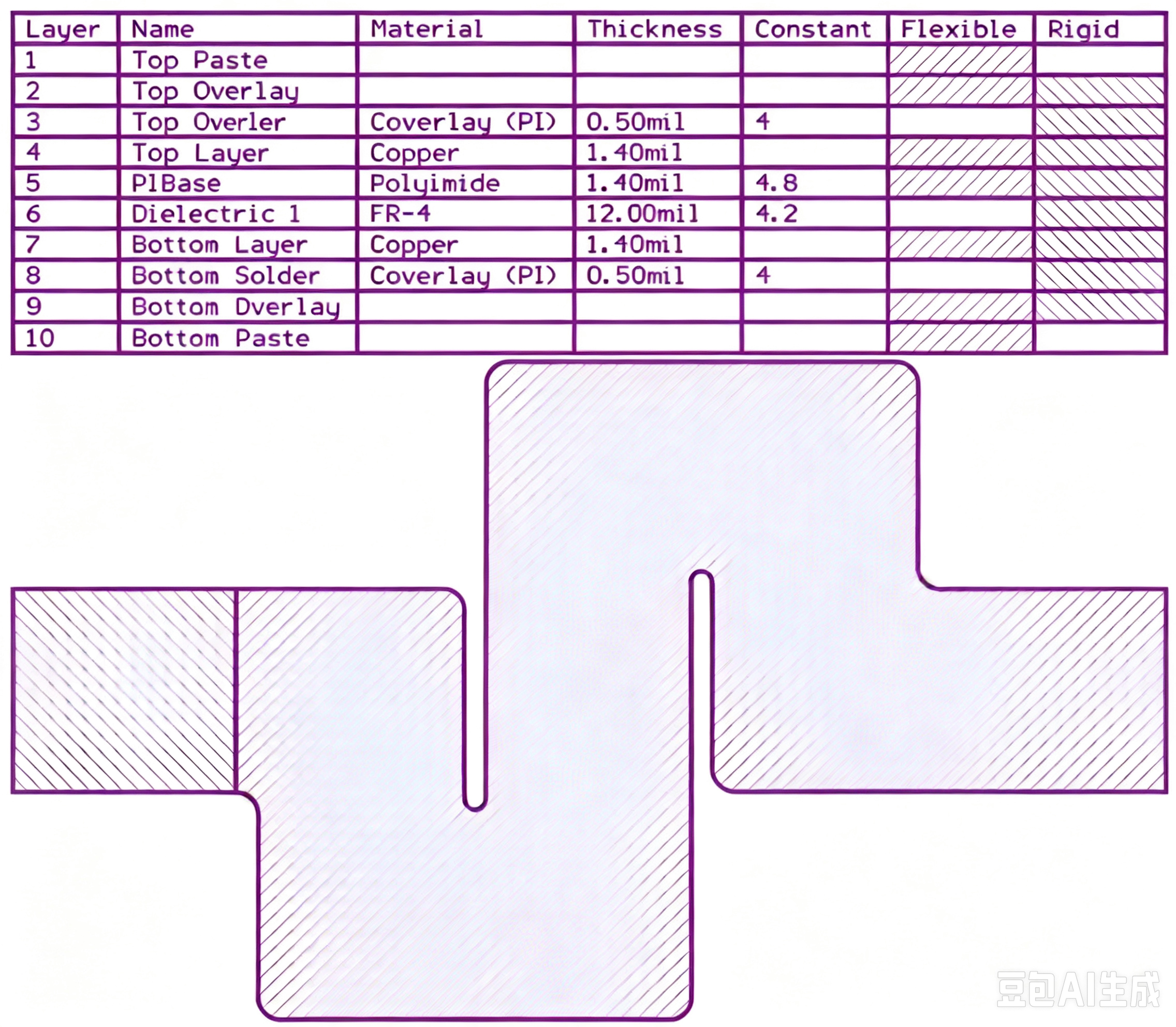
Each additional cycle adds roughly one and a half to two days of production time, which is where the arithmetic becomes uncomfortable. A three-stage board carries four cycles where a plain multilayer board carries one, so the schedule penalty before any yield loss is considered already runs to several days. That penalty appears in every quotation, whether or not the design actually needed the density.
The cycles also compound risk rather than simply adding to it. Every press operation introduces a small alignment error between the layers already present and the new pair, and those errors accumulate. By the time the outer layers are added, the registration window available for the finest features has narrowed, so the process must hold tighter tolerances to achieve the same result that a simpler stackup would reach easily.
Where Yield Is Lost
Yield loss in a high-stage build-up comes from the interaction of several process steps. The drilled holes in a build-up layer are small, so desmear and plating have less margin than in a through hole of conventional size, and the plating must reach the bottom of a blind feature without voids. If the dielectric surface is not prepared correctly, adhesion between the plated copper and the underlying layer suffers, and the connection may pass an electrical test yet fail later under thermal cycling.
Alignment is the second source. Each stage must be registered to the layers beneath it, and the registration error of a four-cycle construction is the sum of the errors of each press. When the pad and the capture pad beneath it drift out of position, the effective annular ring shrinks, and a design that was marginal on the drawing becomes a yield problem in production. This is why a build-up order should be evaluated against the process capability of a specific supplier, not against a generic rule.
Trading Stackup Against Package Pitch
The need for a high build-up order usually originates in one place: the escape routing from a fine-pitch ball grid array. If the pitch is small enough that the inner rows cannot be reached on the available layers, blind and buried via structures become the only way out, and the stackup follows. Changing the pitch changes the whole equation, which is why package selection and stackup selection should be made together rather than sequentially.
A common optimisation is to accept a larger pitch on the device and give up a small amount of board area in exchange for a simpler stackup. In one representative case, a fourteen-layer four-stage design was reduced to a twelve-layer two-stage construction, cutting one lamination cycle and eliminating much of the blind via content. Lead time fell from thirty days to fourteen and cost fell sharply, with the electrical requirements still met. The lesson is not that density is unnecessary, but that it should be paid for only where it is needed.
Checks Before Release
Before a stackup is committed the design should answer three questions. How many lamination cycles does the build-up order require, and is that reflected in the schedule? Is every blind and buried via structure actually necessary for an escape, or is it there because a via was easier to place than to move? And does the design tolerate the registration error that the supplier’s process capability implies at the finest feature size?
Documenting the answer is as important as finding it. A stackup drawing that states the build-up order, the dielectric thickness of each layer, the via types and the impedance targets removes the ambiguity that leads to a supplier quoting one construction and building another. The broader options for high-density construction are described in high density interconnect design and in any layer HDI, while the via filling and plating processes that support them are covered in PCB via plugging. A manufacturability analysis run on the design before release, covering via order, hole spacing and stackup, is far cheaper than discovering the problem in the fabrication queue, and the dimensional limits that apply are collected in PCB manufacturing tolerances.
Process Control and Verification
Reviewing the design before the data is released is far cheaper than correcting it after the panel is in the tank, because every step downstream inherits the decision made at the front end. Where a value sits close to a process limit, the drawing should say so, since the shop can then open the process window rather than working to a nominal figure that carries no tolerance.
The measurements that matter are the repeatable ones: conductor width and spacing, annular ring, finished hole size, plating thickness and surface finish are all verifiable on a coupon that travels with the panel. Documenting the assumption is part of the design work, and a short note on the drawing prevents a question that would otherwise arrive a day later and cost a day of schedule.
FAQ
Is a higher build-up order always better for density? No. It buys routing channels at the cost of lead time, yield risk and price. The right order is the lowest one that still allows every net to escape, so the escape analysis should come before the stackup decision.
Why does a two-stage board need three lamination cycles? Each stage on each side is a separate press and plating operation, and the count in the notation refers to the stages, not the presses. Two stages per side require three cycles in total, and three stages per side require four.
Can a high-stage stackup be fixed after the design is complete? Sometimes, by reducing the device pitch or by re-planning the escape routing to remove dependence on blind vias. Both changes are far easier to make before the layout is finished.