HDI PCB Technology and Microvia Design Rules
A high-density interconnect board is not simply a multilayer board with more layers. It is a board whose interconnect is dense enough that ordinary through-hole vias can no longer serve every connection, so the design moves to smaller holes, finer features and vias that span only the layers they need. That shift changes the stack-up, the fabrication sequence, the design rules and the cost model at the same time.
This article explains what makes a board HDI, how microvias and stacked via structures are built, and which design rules decide whether the board can be manufactured at the price you expect.
What Makes a Board HDI
The threshold is feature density rather than a particular number of layers. A board is treated as HDI when the pad pitch, the trace width and the via diameter fall below what mechanical drilling can support, which in practice means laser-drilled microvias of about 0.15 mm, traces of 0.075 mm, and pad pitches below 0.4 mm.
The driving force is component packaging. Fine-pitch ball grid arrays and chip-scale packages present several hundred connections in an area the size of a fingernail, and escaping those connections on a conventional board would require far more layers than the product can afford. HDI solves the escape problem by allowing vias inside pads and by letting the outer layers carry much more routing than they otherwise could.
Microvias and Laser Drilling
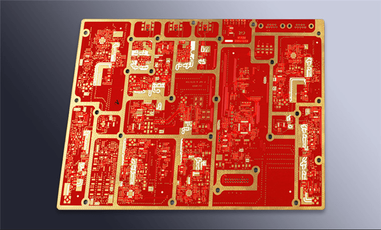
A microvia is formed by a laser rather than a drill bit. It is typically 0.05 to 0.15 mm in diameter and connects only adjacent layers, with a depth no greater than its diameter for reliable plating. That aspect ratio constraint drives everything else: a via deeper than it is wide cannot be plated uniformly, and the thin barrel becomes a latent open circuit that passes electrical test and fails in the field.
Laser drilling works because the beam is absorbed by the copper of the target layer and stops there, which is why a microvia must land on a copper pad rather than on bare laminate. That capture pad has to be large enough to tolerate the registration error of the laser and small enough to leave routing room on a layer that is already congested.
Blind and Buried Via Structures
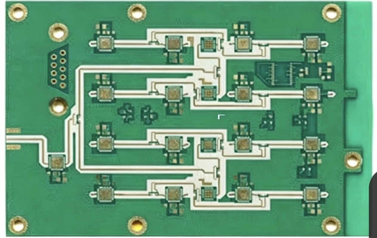
Once microvias exist, the layer stack-up can be organised into via structures that never pass through the whole board. A blind via reaches from an outer layer to an inner layer, while a buried via connects inner layers without touching either surface. Because they consume pad area only on the layers they touch, they free routing space on every layer they skip.
The manufacturing consequence is sequential lamination. Each lamination cycle can create only one set of these structures, so a stack with buried vias plus microvias on both outer surfaces needs several passes through the press. That sequence, not the laminate, is the dominant cost driver on an HDI board.
HDI Stack-Up Families
Most HDI boards fall into a few recognisable families. The simplest is a one-level structure, where microvias exist only between the outer layer and the first inner layer. A two-level structure stacks a second microvia on top of the first, which needs a copper-filled and planarised via to provide a landing surface.
Stacked microvias occupy almost no surface area and are the densest option, but they concentrate mechanical stress in one place and are the most demanding to build. Staggered microvias spread the same connections over two positions and are more forgiving, at the cost of more surface area per connection. Any-layer structures go further still, allowing a via between any two adjacent layers anywhere in the board.
Design Rules That Matter
Capture pad diameter, antipad clearance and the distance from a microvia to the nearest trace are the rules that decide yield. A typical starting point is a capture pad about 0.1 mm larger than the via diameter, with a clearance to surrounding copper that respects the voltage between the nets. On a dense board these clearances consume most of the available area, so they must be budgeted before routing rather than checked afterwards.
Via in pad requires copper filling and plating over the fill, or the solder will wick down the hole during reflow and leave a void under the component. The via filling process in HDI boards explains why the fill has to be planar before the pad can be used reliably. Where the board combines buried and blind structures, the via structure selection guide is a useful check on whether the chosen stack is buildable at the required layer count.
Cost and When It Pays Off
HDI is expensive per unit area, and the price rises stepwise as lamination cycles are added. The justification is almost always total system cost rather than board cost: an HDI board can be smaller, which shrinks the enclosure, the connector count and the assembly cost, and it can support packages that a conventional board cannot route at all.
The decision is therefore not whether HDI is better in the abstract but whether the product’s density requires it. Products where the largest package can be escaped with ordinary vias rarely benefit. Products built around a fine-pitch processor with a dense memory interface usually have no alternative.
A useful way to test the decision is to count the layers the design would need without HDI and price both versions. If the conventional board needs ten layers and a larger outline, the HDI version at six layers frequently wins on total cost even though the laminate itself is more expensive. If the conventional board closes at eight layers within the same footprint, the HDI premium rarely pays back.
Testing and Yield
Fine features reduce the margin for every process step, so testing has to look inside the board rather than only at its surface. Automated optical inspection catches surface defects, X-ray inspection reveals voided or incomplete via barrels, and flying-probe or fixture test confirms continuity on the finished article. A layer count and stack review before release is the cheapest way to avoid discovering that the design needs one more lamination cycle than the budget allows.
Coupon testing deserves particular attention. Impedance coupons, via chains and thermal stress coupons are built alongside the panel and sacrificed, and they are the only practical way to confirm that the plating thickness and the dielectric heights match the design. When yield drops, the coupons tell you which process drifted.
FAQ
How many microvia levels does a typical phone board use? Consumer handset boards commonly use two to three levels, with staggered or stacked microvias in the densest areas and ordinary vias everywhere else. The stack is usually asymmetric in density but symmetric in construction, so the lamination sequence stays manageable. The number of levels follows from the escape requirement of the densest package, not from a target figure chosen in advance.
Can microvias be placed anywhere on the board? They have to land on a capture pad on a copper layer, with the clearance rules respected, and they should not be placed over a plane split or near a board edge where thermal stress concentrates. Within those limits they can be placed wherever the routing needs them.
Is HDI worth it for low volumes? Usually not, because the tooling and lamination setup dominate the cost. Low-volume designs often do better with a conventional multilayer board, a slightly larger package, or a small amount of manual routing assistance at the assembly stage. Where the density is driven by a single fine-pitch device, a common compromise is to keep the conventional stack and place that one device on a small interposer built with HDI rules.