Heavy Copper PCB Manufacturing: Key Processing Considerations
Heavy Copper PCB technology is widely used in electric vehicles, industrial power supplies, high-power converters, and other applications that require high current-carrying capacity and effective heat dissipation. Compared with conventional printed circuit boards, heavy copper PCBs use significantly thicker copper foil, which creates additional challenges throughout the manufacturing process.
From material selection and process control to final quality inspection, every manufacturing stage requires careful attention to the characteristics of thick copper. Understanding these key considerations can help manufacturers improve dimensional accuracy, structural reliability, electrical performance, and long-term service life.
1. Material Selection: Matching Electrical Performance and Manufacturing Requirements
Material selection is one of the first considerations in Heavy Copper PCB Manufacturing. The PCB substrate and copper foil must provide the required electrical and mechanical performance while remaining compatible with the manufacturing process.
Substrate and Copper Foil Compatibility
The bonding strength between thick copper foil and the PCB substrate is critical. Materials with appropriate resin content and good thermal stability should be selected to reduce the risk of copper delamination during high-temperature processes such as soldering and lamination.
Copper foil ductility should also match the intended manufacturing process. If the copper does not have sufficient elongation, cracks may occur during bending or forming operations, potentially affecting the electrical conductivity and mechanical reliability of the finished board.
For demanding applications, manufacturers should evaluate the compatibility of the substrate, copper thickness, thermal characteristics, and mechanical requirements before production.
Materials for High-Power and High-Temperature Applications
Heavy copper PCBs used in high-power environments, such as electric vehicle motor controllers, require materials capable of handling elevated operating temperatures.
Depending on the application, high-temperature substrate materials, including modified epoxy systems or polyimide-based materials, may be considered. Copper foil with appropriate surface treatment can also help reduce oxidation and corrosion during long-term operation.
For applications exposed to frequent mechanical vibration, such as industrial power modules, the fatigue resistance of the substrate and copper structure should also be evaluated. Proper material selection can help reduce the risk of circuit cracking caused by repeated mechanical stress.
2. Manufacturing Process: Controlling Critical Processing Steps
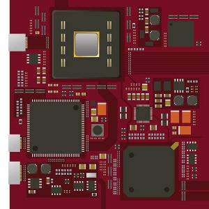
The manufacturing process for a Thick Copper PCB must be adjusted according to the characteristics of thick copper foil. Etching, lamination, drilling, and board forming are particularly important because conventional processing parameters may not provide the required results.
Precise Etching Control
Etching thick copper is more challenging than processing standard copper thicknesses. Etching solution concentration, temperature, and spray pressure must be carefully controlled to maintain consistent results.
Because thicker copper generally requires longer or more carefully controlled etching conditions, excessive lateral etching can affect trace geometry and dimensional accuracy.
Manufacturers may optimize the process through staged or controlled etching approaches to reduce excessive side etching and maintain the required trace width and spacing.
After etching, thorough cleaning is also important. Residual etching chemicals should be removed promptly to reduce the risk of surface oxidation and other potential defects.
Lamination and Interlayer Bonding
Multilayer heavy copper PCBs require careful control during lamination.
Thick copper structures create larger gaps and require sufficient resin flow to achieve reliable interlayer bonding. Lamination temperature and pressure should therefore be properly controlled so that the resin can flow and fill the required areas without creating voids.
For boards using particularly thick copper structures, a staged lamination approach may be considered. Pre-laminating the copper and substrate before the final lamination process can help improve resin filling and reduce the possibility of trapped air.
Cooling after lamination should also be properly controlled. Excessively rapid cooling can create thermal stress and increase the risk of PCB warpage.
Drilling and Board Forming
Drilling heavy copper PCBs can be more demanding because the increased copper thickness places additional stress on drilling tools.
Improper drilling conditions may result in burrs, rough hole walls, excessive tool wear, or other quality issues. High-hardness carbide drill bits and appropriate drilling parameters should be selected according to the copper thickness and board construction.
Cooling and lubrication can also help control heat generation and reduce copper debris accumulation during drilling.
For board forming operations such as CNC routing, appropriate cutting tools and processing parameters should be used to reduce edge chipping and maintain dimensional accuracy.
3. Quality Inspection: Controlling Risks Throughout the Manufacturing Process
Quality control is especially important for High-Current PCB applications because defects in copper structures, holes, insulation, or interlayer bonding can directly affect electrical and mechanical performance.
Inspection should cover the major risk points throughout PCB fabrication rather than relying only on final visual inspection.
Appearance and Dimensional Inspection
High-resolution optical inspection equipment can be used to check trace edges and identify potential issues such as burrs, incomplete etching, or irregular circuit geometry.
Critical dimensions, including trace width and spacing, should also be measured to verify that they meet the specified design requirements.
For multilayer heavy copper boards, additional inspection methods may be required to evaluate interlayer bonding and identify potential voids or delamination.
Mechanical Performance Verification
Some heavy copper PCB applications may involve bending or mechanical stress. In these cases, mechanical testing can help verify the bonding strength between the copper foil and substrate.
The test method should be selected according to the actual application requirements and product specifications.
Electrical Performance Testing
Electrical testing is essential for verifying the performance and reliability of heavy copper circuits.
Typical testing may include:
- Continuity testing
- Insulation resistance testing
- Electrical connection verification
- Current-carrying capability testing
For High-Power PCB applications, current-carrying performance is particularly important. The PCB should be evaluated under the specified operating current to ensure that excessive temperature rise does not compromise reliability.
4. Why Process Control Matters for Heavy Copper PCBs
Heavy copper PCB manufacturing is a comprehensive process involving material engineering, copper processing, lamination technology, mechanical processing, and electrical testing.
Compared with standard PCBs, the increased copper thickness can affect etching behavior, resin filling, drilling conditions, thermal stress, and dimensional stability. As a result, manufacturing parameters should be established according to the actual copper thickness, PCB structure, material system, and application requirements.
A professional manufacturing process should focus on:
- Appropriate copper and substrate selection
- Controlled etching parameters
- Reliable lamination conditions
- Suitable drilling tools
- Accurate board forming
- Strict dimensional inspection
- Electrical performance verification
- Process traceability and quality control
5. Heavy Copper PCB Manufacturing for High-Power Applications
Heavy copper technology is particularly valuable when PCB designs require high current capacity, efficient heat dissipation, and robust electrical connections.
Typical applications include:
- Electric vehicle power electronics
- Motor controllers
- Industrial power supplies
- Power converters
- Battery management systems
- Energy storage equipment
- Industrial control systems
- High-current power modules
In these applications, the PCB is not simply an electrical interconnection platform. Copper thickness, thermal performance, substrate selection, circuit geometry, and manufacturing quality can all influence the final system’s reliability.
For projects requiring both PCB fabrication and assembly, integrating manufacturing with PCB Assembly Services can also simplify supplier coordination and production management.
6. How to Improve Heavy Copper PCB Manufacturing Quality
Improving the quality of heavy copper PCBs requires systematic control from engineering design through final inspection.
Optimize the PCB Design
The circuit layout should consider copper thickness, current requirements, thermal distribution, trace geometry, hole structures, and manufacturing limitations before fabrication begins.
Professional PCB Design & Layout support can help identify potential manufacturing issues at the engineering stage.
Select Materials According to Application Requirements
Substrate materials, copper foil, surface treatments, and other materials should be selected according to operating temperature, current requirements, mechanical stress, and environmental conditions.
Control Critical Manufacturing Parameters
Etching, lamination, drilling, routing, and other processes should use parameters appropriate for heavy copper structures rather than simply applying standard PCB manufacturing settings.
Strengthen Inspection and Testing
Visual inspection, dimensional measurement, mechanical verification, and electrical testing should be integrated into the quality-control process.
For projects that require a complete manufacturing solution, PCB Manufacturing and component sourcing can be coordinated as part of an integrated production workflow.
For assemblies containing high-current power devices, reliable Components Procurement is also important for maintaining component consistency and production stability.
Conclusion
Heavy copper PCB manufacturing requires more than simply increasing the copper thickness of a conventional circuit board. The increased copper structure affects material selection, etching, lamination, drilling, forming, thermal management, and quality inspection.
By selecting compatible materials, optimizing critical manufacturing parameters, controlling interlayer bonding, using appropriate drilling and forming processes, and implementing comprehensive quality inspection, manufacturers can produce reliable heavy copper PCBs for demanding high-current and high-power applications.
GOPCBA provides PCB design, fabrication, component procurement, and assembly solutions for electronic products requiring reliable PCB manufacturing. By integrating engineering and manufacturing capabilities, GOPCBA can support projects from PCB development and prototyping through production.