Heavy Copper PCB Prototyping for Industrial Power Boards
Industrial control systems depend on stable and efficient power distribution. In these applications, the PCB is not simply a carrier for electronic components—it is a critical part of the power architecture. As current loads, operating temperatures, and reliability requirements continue to increase, conventional copper weights may no longer provide sufficient electrical and thermal performance.
A Heavy Copper PCB with copper thicknesses of 2 oz or more offers a practical solution for high-current industrial power applications. Its increased copper thickness improves current-carrying capability, thermal dissipation, mechanical strength, and long-term electrical reliability.
However, manufacturing and prototyping heavy copper boards is considerably more demanding than producing standard PCBs. Copper thickness affects etching, drilling, plating, lamination, dimensional stability, and thermal management. A carefully controlled prototype process is therefore essential before moving into volume production.
Why Heavy Copper PCBs Are Used in Industrial Power Applications
Industrial power electronics often operate under high current, high voltage, continuous-load, and elevated-temperature conditions. Standard PCB structures may experience excessive temperature rise or conductor stress when subjected to demanding electrical loads.
A heavy copper design provides a thicker conductive path, allowing the PCB to handle greater current while reducing resistive losses. The additional copper also improves heat spreading and contributes to the mechanical strength of the finished board.
Typical applications include:
- Industrial motor controllers
- Power conversion equipment
- Industrial automation systems
- Energy storage equipment
- Power supplies
- Battery management systems
- Renewable energy equipment
- High-current control systems
For complex industrial electronics, heavy copper technology can be combined with multilayer structures, controlled impedance, high-TG materials, and other advanced manufacturing technologies. A professional PCB Manufacturing process is essential when several performance requirements must be achieved simultaneously.
Heavy Copper PCB Prototyping Process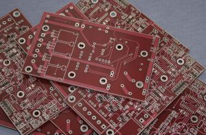
Prototype production provides an important opportunity to verify the electrical, mechanical, and thermal performance of a heavy copper design before committing to larger production volumes.
1. Design Review and Specification Confirmation
The first step is to establish all critical board specifications.
These typically include:
- Copper weight, such as 2 oz, 3 oz, or higher
- PCB thickness
- Number of layers
- Board dimensions
- Base material
- Minimum trace width and spacing
- Hole diameter
- Surface finish
- Solder mask requirements
- Operating voltage
- Expected current load
- Thermal requirements
- Environmental conditions
For industrial applications, engineers should also identify requirements related to temperature, vibration, humidity, insulation, and long-term operating conditions.
A complete engineering review helps identify manufacturing risks before fabrication begins. When necessary, design-for-manufacturing analysis can be used to evaluate trace geometry, stack-up, hole structures, and production feasibility. Professional PCB Design support can help optimize the design before it enters fabrication.
2. Gerber File Review and Manufacturing Engineering
The manufacturing team should carefully review the Gerber files and associated production documentation before starting fabrication.
Heavy copper designs require particular attention to:
- Copper distribution
- Trace width and spacing
- Copper-to-edge clearance
- Hole-to-copper spacing
- Thermal relief structures
- Layer registration
- Board thickness
- Plating requirements
Uneven copper distribution can create manufacturing and dimensional challenges. Similarly, traces designed for standard copper weights may not be suitable for 2 oz or thicker copper.
An engineering review at this stage helps prevent unnecessary prototype revisions and reduces the risk of discovering manufacturability problems after fabrication has started.
3. Material Preparation and Copper Lamination
The selected laminate must provide sufficient mechanical and thermal stability for the intended application.
Depending on the design, common materials may include standard FR-4, high-TG FR-4, and other application-specific materials. Material selection should consider operating temperature, dielectric performance, mechanical strength, and compatibility with the required copper thickness.
During lamination, temperature, pressure, heating rate, and curing conditions must be carefully controlled.
Heavy copper structures can introduce additional thermal mass and affect resin flow. Poor process control may result in:
- Delamination
- Voids
- Uneven bonding
- Copper lifting
- Dimensional instability
Proper material selection and lamination control therefore have a direct influence on long-term board reliability.
4. Pattern Transfer and Heavy Copper Etching
Etching is one of the most challenging stages in heavy copper PCB manufacturing.
As copper thickness increases, maintaining accurate trace geometry becomes more difficult. Conventional etching parameters may cause excessive undercutting or uneven conductor profiles.
A controlled heavy copper etching process must balance:
- Etching speed
- Copper thickness
- Line width
- Line spacing
- Etchant concentration
- Temperature
- Exposure time
The objective is to achieve accurate conductor geometry while minimizing over-etching and residual copper.
For high-current designs, maintaining the intended conductor cross-section is especially important because it directly affects resistance, current capacity, and thermal performance.
5. Drilling and Hole Wall Treatment
Heavy copper boards and thicker overall PCB structures can require optimized drilling parameters.
CNC drilling must maintain accurate hole position while preventing:
- Hole wall damage
- Burr formation
- Resin smear
- Drill deviation
- Excessive tool wear
After drilling, hole cleaning and desmear processes prepare the hole walls for subsequent copper metallization.
For plated through-holes, reliable copper deposition inside the hole is essential because the plated barrel becomes an important electrical connection between PCB layers.
When the board incorporates complex multilayer structures, blind or buried vias may also be considered depending on the design requirements.
6. Copper Plating and Electrical Connection
After drilling and hole preparation, copper is deposited onto the hole walls to establish electrical conductivity.
Additional electroplating can then increase copper thickness according to the required design and reliability specifications.
For heavy copper boards, plating must be carefully controlled because variations in copper distribution can influence conductor dimensions, hole reliability, and overall board performance.
Quality control should verify:
- Plated copper thickness
- Hole wall quality
- Electrical continuity
- Insulation performance
- Layer-to-layer connections
For demanding PCB applications, manufacturers may combine automated optical inspection, electrical testing, X-ray inspection, and other quality-control methods to verify structural and electrical integrity.
7. Solder Mask and Surface Finishing
After the copper circuitry has passed inspection, solder mask is applied to protect the PCB surface and electrically isolate areas that should not be exposed.
The process generally includes coating, pre-baking, exposure, development, inspection, and final curing.
Surface finishing is then selected according to the application and assembly requirements. Common options include:
- ENIG
- HASL
- Lead-free HASL
- OSP
- Immersion silver
- Immersion tin
- ENEPIG
The surface finish affects oxidation resistance, solderability, contact reliability, and storage performance.
For industrial power electronics, the selected finish should be evaluated together with the assembly process and expected operating environment.
8. Final Testing and Dimensional Inspection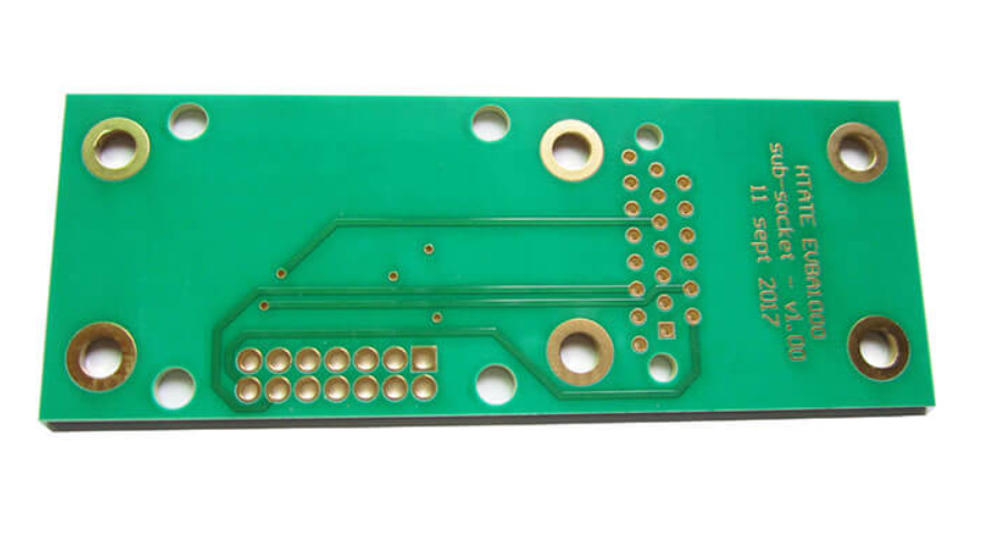
Prototype testing should go beyond a basic visual inspection.
For industrial power boards, important verification items may include:
Electrical Testing
Electrical testing verifies circuit continuity and insulation performance. It helps identify open circuits, shorts, and other electrical defects before the prototype is released for system testing.
Dimensional Inspection
Board length, width, thickness, hole position, hole diameter, and other mechanical dimensions should be measured against the engineering drawings.
Copper Thickness Verification
Copper thickness should be verified to ensure the board meets the specified current-carrying requirements.
Thermal Verification
Where applicable, prototype boards should be tested under representative current loads to evaluate temperature rise and heat distribution.
High-Voltage Testing
For high-voltage industrial applications, dielectric withstand and insulation performance may require additional verification according to the product’s electrical safety requirements.
Combining PCB fabrication with assembly and testing can also shorten the development cycle by allowing engineers to evaluate the complete electronic assembly rather than the bare board alone. Low-volume production is particularly useful for engineering validation and product testing.
Key Considerations When Prototyping Heavy Copper PCBs
Match Copper Weight With the Application
The copper weight should be selected according to the expected current, temperature rise, conductor geometry, and available board space.
Using unnecessarily thick copper may increase manufacturing complexity and cost, while insufficient copper may result in excessive temperature rise and electrical losses.
Optimize Copper Distribution
Large differences in copper density between different areas of a board can contribute to manufacturing and thermal challenges.
A balanced copper distribution should therefore be considered during the design stage.
Consider Thermal Management
Heavy copper improves heat conduction, but it should not be treated as a complete thermal-management solution.
The PCB design may also require thermal vias, heat sinks, copper planes, appropriate component placement, and optimized airflow.
Verify Manufacturing Tolerances
Thicker copper and heavier board structures can make dimensional control more challenging. Critical tolerances should be defined clearly before production.
Test Prototypes Under Realistic Conditions
A prototype should be evaluated under operating conditions that reasonably represent the final product.
Testing current load, temperature rise, voltage withstand, vibration, and other application-specific requirements can reveal problems that cannot be identified through visual inspection alone.
Why Prototype Validation Matters Before Mass Production
Moving directly from PCB design to mass production can create unnecessary risk, especially when the design uses heavy copper, complex multilayer structures, or demanding electrical specifications.
Prototype production provides an opportunity to validate:
- Electrical performance
- Current-carrying capability
- Thermal behavior
- Mechanical dimensions
- Hole reliability
- Surface finish
- Assembly compatibility
- Manufacturing repeatability
After prototype validation, engineering teams can make targeted improvements before transitioning to larger production quantities.
For projects requiring both fabrication and assembly, an integrated manufacturing partner can simplify communication between PCB fabrication, component sourcing, SMT/THT assembly, inspection, and final testing.
Custom Heavy Copper PCB Manufacturing for Industrial Applications
Heavy copper PCB prototyping is a specialized manufacturing process that requires careful coordination between PCB design, material selection, etching, drilling, plating, thermal management, inspection, and testing.
For industrial power electronics, the objective is not simply to produce a board with thicker copper. The entire PCB structure must be engineered around the electrical load, thermal requirements, mechanical environment, and expected service life.
A professional Custom PCB Manufacturing partner can provide engineering review, DFM analysis, material selection, fabrication, inspection, and prototype-to-production support through a controlled manufacturing workflow.
For projects that require rapid validation or small production quantities, PCB Prototyping and low-volume manufacturing provide an efficient way to verify the design before committing to larger production runs.
By combining appropriate copper thickness, optimized PCB geometry, reliable materials, controlled manufacturing processes, and comprehensive testing, engineers can develop High Current PCB solutions capable of supporting demanding industrial power applications with stable electrical and thermal performance.