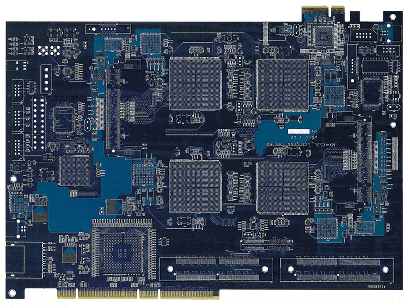
High Frequency Filter PCB: Layout and Tolerance Control
A filter is one of the few circuits whose performance depends on the physical dimensions of the board rather than only on the components. In the lower megahertz range a filter is built from discrete parts, but as the frequency rises the traces become resonators, the pad capacitance becomes part of the tuning and the dielectric constant of the laminate sets the centre frequency. A high frequency filter PCB therefore has to be designed and measured as a structure.
Filter Types and What They Demand
Low pass filters remove harmonics after an amplifier, band pass filters select a channel in a receiver front end, and notch or band stop filters reject a specific interferer. Each has a topology that translates into a physical pattern, and each has a different sensitivity to manufacturing variation.
The pattern may be a series of coupled lines, a stub arrangement or a set of lumped elements that behave as resonators at the operating frequency. In every case, the electrical length of the elements is fixed by the wavelength on the board, which depends on the dielectric constant of the material and on the geometry of the line.
Material Choice and Dielectric Constant
The dielectric constant of the laminate sets the wavelength, and therefore sets how long a resonator has to be. A material with a stable dielectric constant holds the centre frequency across temperature and batch, which is what a narrow band filter needs to stay inside its specification.
Stability matters more than the absolute value here. A design can accommodate any known dielectric constant, but it cannot accommodate one that drifts. This is the reason filter work moves to low loss, low variation laminates earlier than other circuits, and the material comparison is the one discussed in the general treatment of a microstrip and stripline structure.

Distributed and Lumped Approaches
A distributed filter uses transmission line sections as its resonators. It is simple to fabricate and has no component losses, but the elements become physically large at lower frequencies and the design occupies considerable board area.
A lumped element filter uses inductors and capacitors whose values are small enough to be practical at the operating frequency, and it fits into a fraction of the area. The price is sensitivity: the parasitic capacitance of the pads and the self resonance of the components become part of the response, and the design has to be simulated with those parasitics included from the first iteration.
Ground Plane Continuity
The ground plane is part of the filter, not a backdrop. A distributed filter’s resonators couple to the plane beneath them, and any discontinuity in that plane changes the coupling and shifts the response. A slot for a connector or a plane split under the filter can destroy the stop band entirely.
Coplanar structures rely on the top side ground as well, and their performance depends on the stitching vias that tie the two ground layers together at a consistent spacing. Placing those vias at a regular interval along the structure keeps the two grounds at the same potential and suppresses the parallel plate mode between them, an idea that appears in the same form in EMI suppression design principles.
Tolerance and Sensitivity
Every dimension on a filter has a tolerance, and the response is the sum of their effects. Etch tolerance changes the width of a resonator, dielectric thickness tolerance changes the impedance, and the dielectric constant varies within a batch. A narrow band design amplifies all of these.
Simulation should therefore be run at the tolerance corners, not only at nominal. A filter that meets its insertion loss at nominal and fails it with the etch at the low limit is a design that will lose yield, and the fix, which is a slightly wider band with more margin, is easier to apply before the board is released. Tolerance is also why the loss budget should be expressed in terms of the whole chain rather than the filter alone.
Component Parasitics and Placement
Where lumped elements are used, the pads that connect them are part of the circuit. A pad of half a millimetre adds capacitance that shifts a resonator, and a via adds inductance that shifts it further. Keeping pads small, placing components symmetrically and using short ground returns with via arrays all reduce the deviation from the simulated design.
Component selection has to consider self resonance as well. A capacitor whose resonance falls near the operating frequency is inductive above that point and will not behave as the designer intended. The chosen parts should have their resonance well above the band, and the same part number should be used in production so that the response does not move.
Measurement Practice
A filter is verified with a network analyser, and the connection to the analyser has to be calibrated at the reference plane of the board. Measuring through a connector and a cable without that calibration includes the fixture in the result, which is often larger than the effect being investigated.
The key measurements are insertion loss in the pass band, return loss at the ports and rejection in the stop band, and they should be recorded across frequency rather than at a single point. Comparison against the simulation is what shows whether the discrepancy comes from the material, the etch or the assembly.
Fabrication Considerations
Filter boards ask more of the fabricator than ordinary digital boards. Etch tolerance on narrow lines is critical, the layer to layer registration affects coupling, and the plating must be consistent because the loss depends on the conductor surface. A supplier used to impedance controlled work will have the process control that this requires.
The stackup should be specified with the filter in mind, because the dielectric thickness under the resonator is part of the electrical design. Where the board carries both filters and digital circuitry, the filter layers are usually placed against a solid reference and the digital layers kept separate, which is the reasoning behind the guidance in layer stackup from one to eight layers.
Applications and Trade Offs
Filters built on the board appear in radio front ends, in harmonic suppression after power amplifiers, in receiver channel selection and in diplexer arrangements that split two bands at a common port. Each of them trades size, loss and selectivity, and the board designer is usually balancing all three against a fixed board area.
The trade is decided by the requirement rather than by preference. Where selectivity is the priority, a higher order filter with more resonators is used and the loss rises with it. Where loss matters more, the order is reduced and the burden moves to the system level. Recording that decision is what prevents a later change from invalidating the whole radio chain.
FAQ
Why did my filter centre frequency shift after fabrication? Almost always the dielectric constant of the delivered laminate or the etched width of the resonators. Measuring the material on a coupon isolates which of the two is responsible.
Can a filter be tuned after assembly? It can be trimmed with small capacitors or by adjusting the pattern, which is common at prototype stage. Production should rely on process control rather than on tuning.
Does the solder mask affect the response? It does, because the coating changes the effective dielectric constant above the trace. The effect is small but repeatable, so the design should be simulated and measured with the same mask condition that production will use.