As electronic systems continue to operate at higher frequencies and data rates, conventional PCB Design practices may no longer be sufficient to maintain stable signal transmission. At microwave and high-speed frequencies, even small changes in trace geometry, dielectric properties, via structure, surface finish, or grounding can affect signal integrity.
A well-designed High-Frequency PCB must therefore control impedance, minimize signal reflections, reduce parasitic inductance and capacitance, and provide predictable electromagnetic-field distribution.
The following guidelines can help designers improve High-Frequency PCB Design performance and reduce problems such as return loss, crosstalk, electromagnetic interference, and excessive signal attenuation.
1. Optimize Transmission-Line Bends
Sharp corners in high-frequency transmission lines can introduce impedance discontinuities and affect the local electromagnetic field.
For this reason, transmission-line corners should be designed with appropriate angles or curved geometries rather than abrupt 90-degree turns. A commonly used approach is to use chamfered corners, such as approximately 45-degree transitions, or smoothly curved traces where appropriate.
The original design recommendation of approximately 4.5° should not be treated as a universal requirement. The appropriate geometry depends on the operating frequency, trace width, stackup, dielectric constant, and manufacturing capability.
For critical microwave traces, electromagnetic simulation or field-solver analysis can be used to evaluate the effect of bends on impedance and Signal Integrity.
2. Use Controlled-Dielectric Materials
Material selection is one of the most important aspects of High-Frequency PCB Design.
High-frequency signals are strongly influenced by the dielectric constant (Dk), dissipation factor (Df), dielectric thickness, copper roughness, and dimensional stability of the PCB material.
High-performance dielectric materials with tightly controlled electrical properties can help designers maintain a predictable electromagnetic field between the signal trace and its reference plane.
When selecting PCB materials, designers should consider:
- Dielectric constant (Dk)
- Dissipation factor (Df)
- Dielectric thickness
- Copper roughness
- Thermal stability
- Dimensional stability
- Moisture absorption
- Frequency-dependent material characteristics
The nominal Dk value alone is not sufficient. For demanding microwave applications, the material’s Dk and Df should be evaluated at frequencies relevant to the actual application.
3. Improve PCB Etching and Trace Geometry Control
Precise trace geometry is essential for Impedance Control.
At high frequencies, impedance depends not only on nominal trace width but also on conductor thickness, dielectric height, copper roughness, etching profile, and the geometry of the trace sidewalls.
During PCB fabrication, designers and manufacturers should control:
- Trace width
- Copper thickness
- Etching compensation
- Sidewall profile
- Undercut
- Conductor spacing
- Dielectric thickness
- Registration accuracy
For high-precision applications, the allowable trace-width tolerance should be established according to the actual impedance requirement and manufacturing capability rather than using a single universal tolerance value.
The overall management of trace geometry is particularly important at microwave frequencies because current distribution is no longer uniform across the conductor.
Why Trace Geometry Matters
At high frequencies, the electromagnetic field becomes highly sensitive to changes in conductor geometry.
A small variation in trace width can change characteristic impedance. Similarly, excessive copper roughness or an inconsistent etching profile can increase conductor loss.
Therefore, high-frequency PCB fabrication requires close coordination between PCB design and manufacturing engineering.
4. Understand the Skin Effect
The Skin Effect is an important consideration in high-frequency circuit design.
As frequency increases, alternating current tends to concentrate closer to the surface of a conductor rather than being distributed uniformly throughout its cross-section.
The effective current-carrying area therefore decreases, which increases AC resistance and conductor loss.
The skin depth can be approximated by:
δ = √(2ρ / ωμ)
where:
- δ is the skin depth
- ρ is conductor resistivity
- ω is angular frequency
- μ is magnetic permeability
As frequency increases, skin depth decreases.
This means that copper surface characteristics become increasingly important in microwave and high-speed PCB applications.
Copper roughness can increase the effective path length of high-frequency current and contribute to additional conductor loss. Therefore, low-profile copper or appropriately treated copper may be beneficial for demanding high-frequency applications.
5. Avoid Unnecessary Leaded Components
Component leads introduce parasitic inductance and capacitance.
At low frequencies, the electrical effect of a component lead may be negligible. At high frequencies, however, even a relatively short lead can become electrically significant.
For this reason, High-Frequency PCB designs generally favor surface-mount components over through-hole components where practical.
Surface-mount components provide shorter electrical paths and can reduce parasitic effects.
For high-frequency signal paths, designers should minimize:
- Long component leads
- Unnecessary wiring
- Large signal loops
- Excessive pad dimensions
- Uncontrolled stubs
- Long transitions between layers
Component placement should also be optimized so that critical signal paths remain as short and direct as possible.
6. Minimize Via-Induced Discontinuities
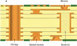
A PCB Via introduces a vertical transition between PCB layers and therefore creates parasitic inductance and capacitance.
Through-hole vias can also create unused via stubs that extend beyond the active signal layer. At high frequencies, these stubs can behave as resonant structures and cause impedance discontinuities.
For sensitive high-frequency signals, designers should therefore minimize unnecessary via transitions.
Where appropriate, consider:
- Blind vias
- Buried vias
- Microvias
- Back-drilled vias
- Shorter via structures
- Optimized antipads
- Proper ground-via placement
The correct solution depends on the PCB stackup, operating frequency, manufacturing capabilities, and cost requirements.
Not every high-frequency design requires microvias or blind vias, but critical signal transitions should always be evaluated for their electrical impact.
7. Provide a Continuous Ground Reference
A properly designed Ground Plane is essential for high-frequency signal integrity.
High-frequency signals return through paths determined by electromagnetic fields and the impedance of the surrounding structure. The return current generally follows the path of lowest impedance, which is often closely associated with the reference plane beneath the signal trace.
A continuous ground plane can:
- Provide a stable signal reference
- Reduce loop area
- Improve impedance control
- Reduce electromagnetic radiation
- Reduce crosstalk
- Improve return-current continuity
Ground planes should not be unnecessarily split beneath high-speed signal traces.
When a signal crosses a plane split or gap, its return current may be forced to take a longer path. This increases loop area and can increase electromagnetic radiation and signal-integrity problems.
8. Use Ground Vias to Control Three-Dimensional Fields
Ground vias can provide low-inductance connections between ground planes and help control electromagnetic fields in multilayer high-frequency structures.
A properly arranged group of ground vias can create a more controlled electromagnetic environment around sensitive transmission lines.
Ground-via placement is particularly important around:
- High-speed signal transitions
- RF connectors
- Coaxial-to-microstrip transitions
- Shielding structures
- Differential signal transitions
- Layer transitions
The spacing between ground vias should be selected according to the operating frequency and physical structure. At higher frequencies, smaller via spacing may be necessary to maintain effective electromagnetic containment.
9. Select an Appropriate PCB Surface Finish
Surface finish can influence high-frequency conductor loss, solderability, and manufacturing reliability.
For demanding high-frequency applications, finishes such as electroless nickel immersion gold (ENIG) or other suitable immersion finishes may be considered depending on the application and required electrical performance.
However, surface finish selection should not be based solely on the assumption that one finish is always better for high-frequency current.
For microwave applications, the thickness and resistivity of the nickel layer in ENIG should be evaluated because nickel has significantly higher resistivity than copper and can contribute to conductor loss.
For extremely high-frequency or low-loss designs, alternative finishes or bare-copper-compatible processes may be evaluated depending on solderability, reliability, oxidation protection, and assembly requirements.
Therefore, surface-finish selection should be made jointly according to electrical, manufacturing, and assembly requirements.
10. Control Solder Mask Effects
Solder mask is an important part of conventional PCB manufacturing, but it can influence high-frequency transmission lines.
A solder mask layer adds dielectric material above the copper trace. Because its thickness and dielectric properties differ from the underlying PCB dielectric, it can change the local electromagnetic field and therefore affect characteristic impedance.
This effect is particularly relevant to exposed microstrip structures.
For critical high-frequency traces, designers should determine whether the solder mask should cover the transmission line or whether a solder-mask-defined keep-out area is more appropriate.
The decision should consider:
- Operating frequency
- Trace geometry
- Required impedance
- Solder mask thickness
- Dielectric properties
- Manufacturing tolerances
For controlled-impedance designs, the PCB manufacturer should know whether the impedance calculation assumes solder mask coverage.
11. Carefully Design Microstrip-to-Coaxial Transitions
The transition between a microstrip transmission line and a coaxial connector is another potential source of impedance discontinuity.
A typical microstrip structure consists of a signal trace on one PCB layer with a reference ground plane beneath it.
A coaxial connector, in contrast, has a three-dimensional electromagnetic structure with a center conductor surrounded by a conductive shield.
The transition between these two structures should therefore be designed carefully.
Potential discontinuities may occur because of:
- Pad geometry
- Ground clearance
- Via arrangement
- Connector launch structure
- Dielectric thickness
- Trace width
- Ground-plane configuration
An optimized connector launch can significantly reduce reflection and return loss.
For high-frequency designs, electromagnetic simulation can be used to optimize the transition geometry before fabrication.
12. Pay Attention to Return Loss
Return loss is an important parameter in high-frequency transmission systems.
Whenever a signal encounters an impedance discontinuity, part of the signal energy is reflected toward the source.
The reflection coefficient can be expressed as:
Γ = (ZL − Z0) / (ZL + Z0)
where:
- Γ is the reflection coefficient
- ZL is the load impedance
- Z0 is the characteristic impedance of the transmission line
A well-controlled transmission system minimizes impedance discontinuities and therefore reduces signal reflections.
This is why trace geometry, vias, connectors, component pads, PCB stackup, and transmission-line transitions must all be considered as part of the same high-frequency interconnect system.
13. High-Frequency PCB Design Checklist
Before releasing a PCB Design for high-frequency fabrication, engineers should review the following items:
- Is the PCB material suitable for the operating frequency?
- Are Dk and Df adequately controlled?
- Is the stackup designed for the required impedance?
- Are critical trace widths properly controlled?
- Has copper roughness been considered?
- Are unnecessary vias and via stubs minimized?
- Are continuous reference planes provided?
- Are return-current paths uninterrupted?
- Are sensitive traces separated from noisy circuits?
- Are connector launches properly designed?
- Has solder-mask influence been evaluated?
- Is the selected surface finish appropriate?
- Are component leads minimized?
- Have critical transitions been simulated or verified?
- Are manufacturing tolerances compatible with the electrical requirements?
Kingda’s Approach to High-Frequency PCB Manufacturing
High-frequency PCB performance depends on the interaction between material selection, PCB Design, fabrication accuracy, surface treatment, layer stackup, and assembly processes.
Kingda can support high-frequency PCB projects by considering these requirements together during the design-for-manufacturing and fabrication stages.
For demanding microwave and high-speed applications, manufacturing consistency is especially important. Trace width, dielectric thickness, copper thickness, registration accuracy, via geometry, surface finish, and material characteristics can all affect final electrical performance.
By aligning PCB design requirements with actual manufacturing capabilities, Kingda can help customers achieve more predictable impedance, better signal integrity, and improved production consistency.
Conclusion
Successful High-Frequency PCB Design requires much more than simply increasing the quality of PCB materials. Transmission-line geometry, impedance control, via structures, grounding, surface finish, solder mask, component selection, and connector transitions must all be considered as part of a complete electromagnetic system.
The Skin Effect also becomes increasingly important as operating frequency rises, making copper surface characteristics and conductor geometry critical factors in controlling insertion loss.
For high-frequency and microwave applications, designers should establish the PCB stackup and transmission-line structure early, maintain continuous reference planes, minimize unnecessary vias and stubs, carefully control trace geometry, and coordinate closely with the PCB manufacturer.
When electrical design and manufacturing capabilities are properly aligned, high-frequency PCBs can achieve more stable impedance, lower signal loss, improved Signal Integrity, and greater overall system reliability.